Supercharge Your Innovation With Domain-Expert AI Agents!

Electronic circuit module

a technology of electronic circuit module and circuit board, which is applied in the direction of transmission, electrical apparatus construction details, basic electric elements, etc., can solve the problems of electronic circuit module size exceeding the total surface area, and the limitation of the total surface area of these electronic circuit boards, so as to reduce the surface area, and reduce the surface area

Inactive Publication Date: 2005-08-18
RENESAS TECH CORP
View PDF14 Cites 18 Cited by
  • Summary
  • Abstract
  • Description
  • Claims
  • Application Information

AI Technical Summary

Benefits of technology

"The present invention provides an electronic circuit module with a reduced mounting area and improved performance. The module includes a module substrate, multiple electronic circuit units, and a surface area smaller than the total surface area of the electronic circuit units. The arrangement of the electronic circuit units on the module substrate allows for a smaller size of the module. The invention also reduces the number of wirings on the module substrate, which helps to decrease the surface area of the module. The module substrate includes a thermal conductive material to improve heat dissipation. The invention further provides a solution for reducing the size of the module without using an expensive multilayered substrate."

Problems solved by technology

However, the electronic circuit module described above, including the conventional module structure disclosed in the patent document 1, has a problem because each electronic circuit unit is arranged in the plane over the module substrate.
The problem is that the electronic circuit module cannot be reduced in size exceeding the total surface area of respective electronic circuit units.
In other words, if the electronic circuit module is reduced in size by improving arrangement on the surface of each electronic circuit unit, the total surface area of these electronic circuit units has a limitation and further reduction in size is impossible.
Therefore, when the number of wirings on the surface of module substrate is reduced by introducing a multilayered for the module substrate in order to avoid increase in the surface area, here rises a problem that the module substrate becomes expensive.

Method used


Image

  • Electronic circuit module
  • Electronic circuit module
  • Electronic circuit module

Examples


first embodiment

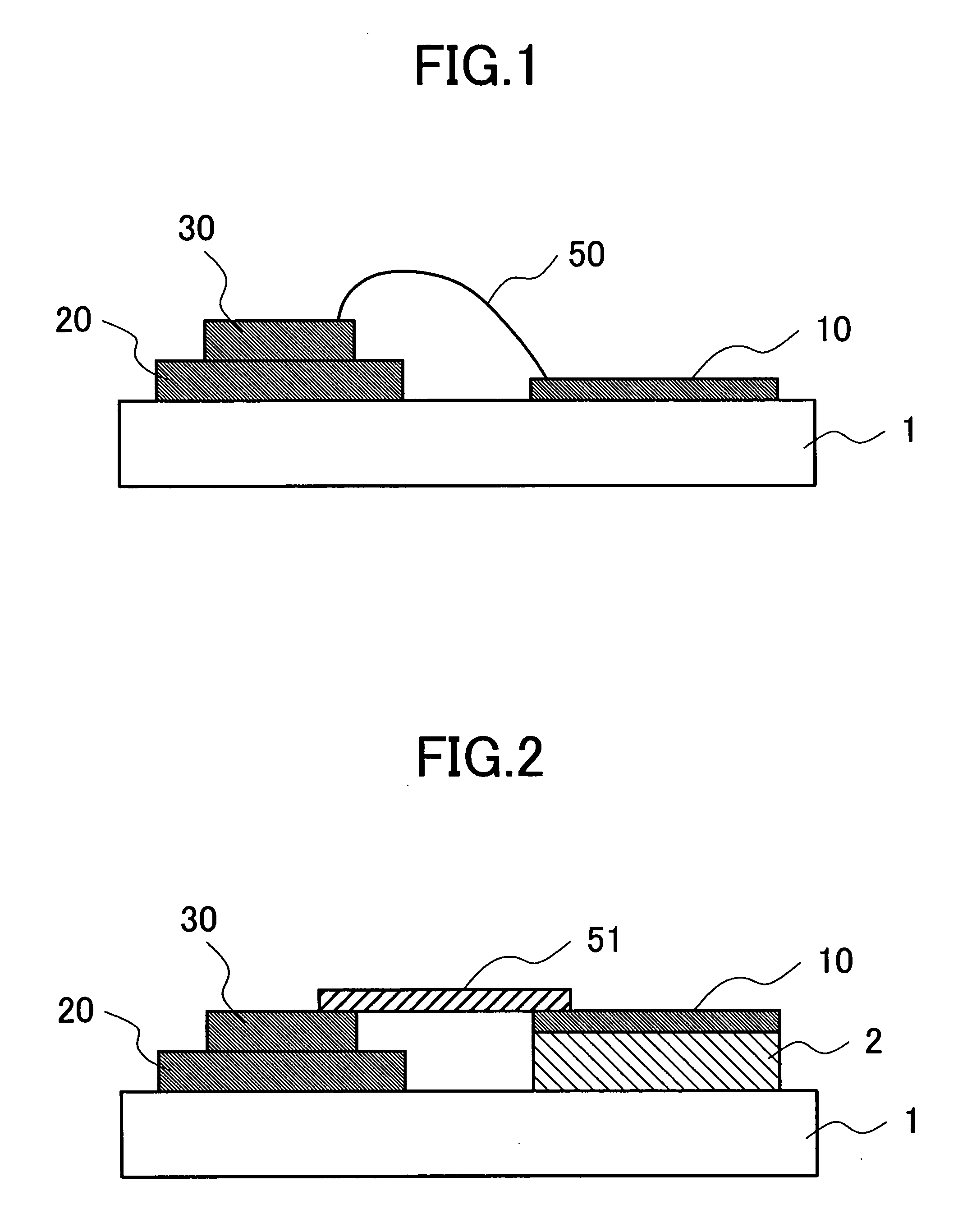
[0052]FIG. 1 is a cross-sectional view illustrating the first embodiment of an electronic circuit module of the present invention. Over a module substrate 1, a first electronic circuit unit 10 which generates a large amount of heat is mounted with the surface (rear surface) on which active devices are not formed placed in contact with the module substrate. In regard to a second electronic circuit unit 20 and a third electronic circuit unit 30 which generate less amount of heat than the first electronic circuit unit, the second electronic circuit unit is mounted to the position different from the first electronic circuit unit over the module substrate, while the third electronic circuit unit is mounted over the second electronic circuit unit, respectively. The electronic circuit module is constituted with provision of these first to third electronic circuit units 10, 20, 30 and the module substrate 1.

[0053] The electronic circuit module is a high-frequency circuit module for GSM (Gl...

second embodiment

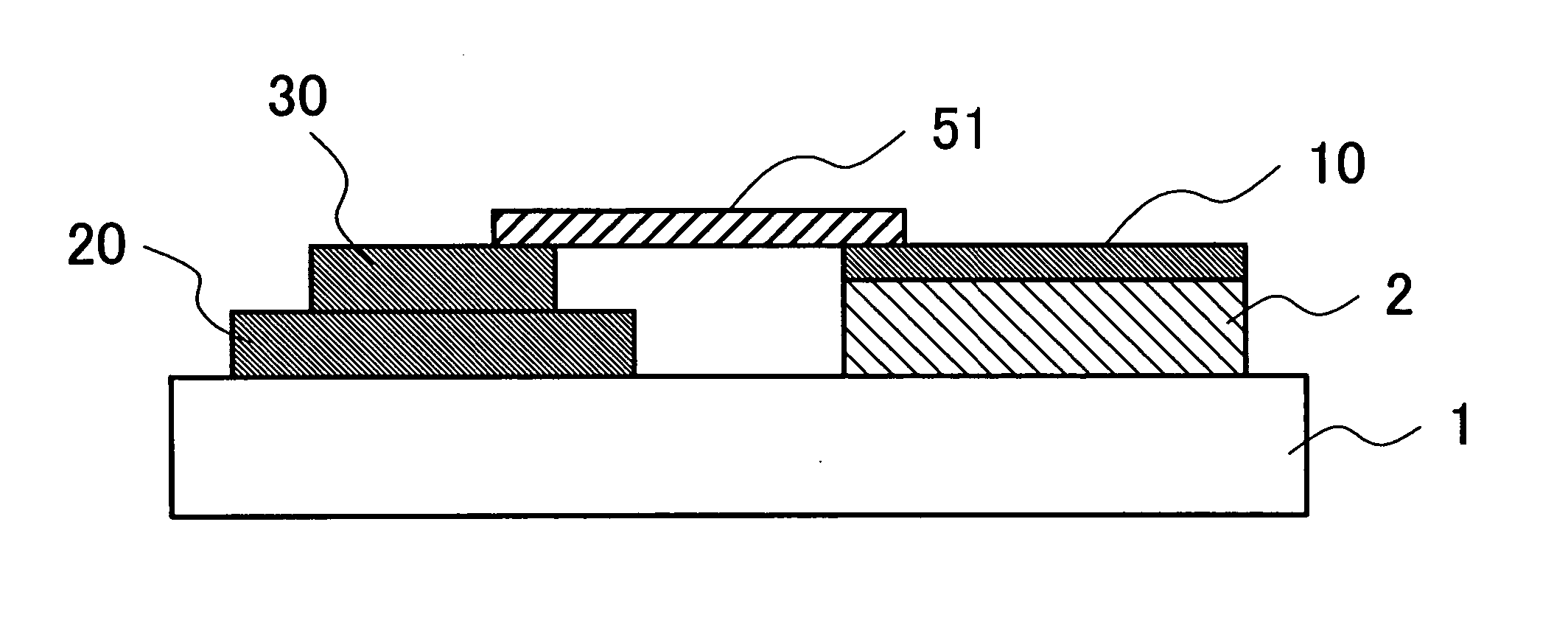
[0062]FIG. 2 is a cross-sectional view illustrating a second embodiment of the electronic circuit module of the present invention. In this embodiment, the electronic circuit module and module substrate identical to that in the first embodiment are used. A thermal conductive material 2 is inserted between the first electronic circuit unit 10 (PA-MMIC) and the module substrate 1 so that the upper surface of the first electronic circuit unit 10 (PA-MMIC) becomes equal in height to the upper surface of the third electronic circuit unit 30 (power control IC). As the thermal conductive material 2, for example, molybdenum (Mo) may be used. This material ensures excellent thermal conductivity and shows a small difference in the thermal expansion coefficient against the first electronic circuit unit 10 (PA-MMIC).

[0063] Like the first embodiment, heat radiation from the first electronic circuit unit 10 (PA-MMIC) is suitably performed, as illustrated in FIG. 11, to a mother board of a cellula...

third embodiment

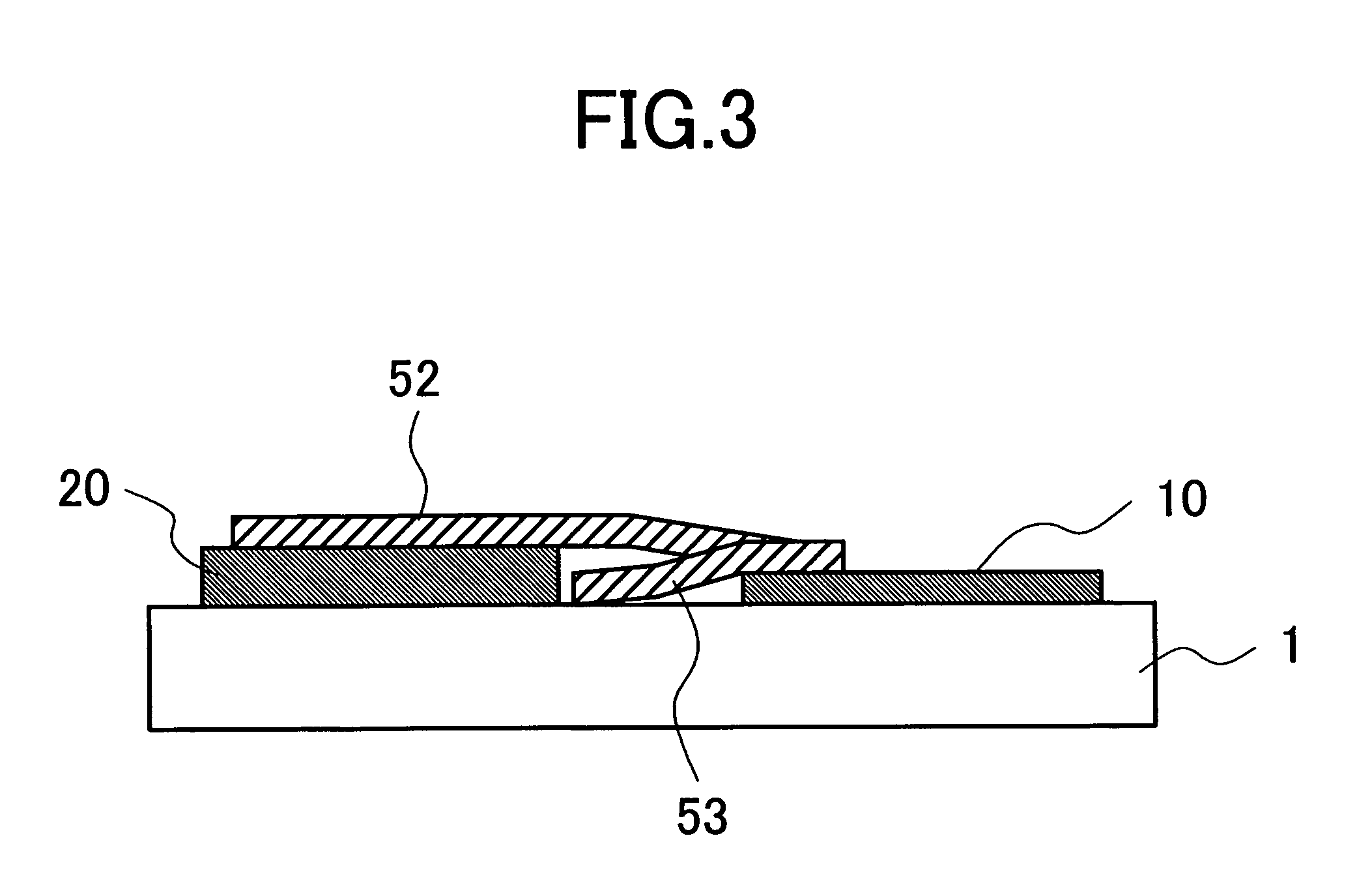
[0068]FIG. 3 is a cross-sectional view illustrating a third embodiment of the electronic circuit module of the present invention. In this third embodiment, the first electronic circuit unit 10 (PA-MMIC), second electronic circuit unit 20 (RF-IC), third electronic circuit unit 30 (power control IC), and module substrate 1 which are identical to that in the first embodiment may be used. However, the second electronic circuit unit 20, for example, may be the RF-IC with the power control function in the structure where the power control IC is integrally formed to a CMOS circuit in the RF-IC. In this case, the electronic circuit unit 20 (RF-IC with the power control function) and the first electronic circuit unit 10 (PA-MMIC) are electrically connected with an inter-unit connection conductor provided over the first auxiliary substrate 52. Moreover, the electronic circuit unit 20 (RF-IC with the power control function) may be mounted on the module substrate 1 with the surface (rear surfac...


PUM


Abstract

An electronic circuit module mounting a plurality of electronic circuit units in which an area thereof can be reduced without increase in the number of module substrate layers while the performance of each electronic circuit unit is not deteriorated. In the electronic circuit module mounting a plurality of electronic circuit units on a sheet of module substrate, a first electronic circuit unit which generates a large amount of heat and a second electronic circuit unit, a third electronic circuit unit which generate less amount of heat than the first electronic circuit unit are mounted. In this case, the first electronic circuit unit is mounted with the surface not forming active device to be in contact with the module substrate and the third electronic circuit unit is mounted over said second electronic circuit unit.

Description

CLAIM OF PRIORITY [0001] The present application claims priority from Japanese application JP 2004-039523 filed on Feb. 17, 2004, the content of which is hereby incorporated by reference into this application. FIELD OF THE INVENTION [0002] The present invention relates to an electronic circuit module in which a plurality of electronic circuit units are mounted and particularly to an electronic circuit module in which electronic circuit units which generate a large amount of heat and the other electronic circuit units are mounted. BACKGROUND OF THE INVENTION [0003] As the technology to realize reduction in size of portable equipment, circuit integration of electronic circuits and formation of electronic circuit module of a plurality of electronic circuit units have been proposed. The circuit integration outstandingly excels in a degree of size reduction but it is difficult from the viewpoint of technology to accommodate devices which require different processes into an integrated cir...

Claims


Application Information

Patent Timeline
Patent Type & Authority Applications(United States)
IPC IPC(8): H01L25/18H01L21/60H01L23/66H01L25/04H01L25/065H01L25/16H04B1/38H05K1/02H05K1/14H05K7/06H05K7/20
CPCH01L23/66H01L24/32H01L24/86H01L25/0652H01L25/16H01L2224/45015H01L2224/48091H01L2224/48137H01L2224/49111H01L2224/49171H01L2224/49175H01L2924/01025H01L2924/01029H01L2924/01078H01L2924/01079H01L2924/10329H01L2924/14H01L2924/1423H01L2924/19041H01L2924/20752H01L2924/3011H04B1/38H05K1/0206H05K1/147H01L24/45H01L24/48H01L2224/48227H01L2924/01006H01L2924/01019H01L2924/01033H01L2924/01042H01L24/49H01L2924/0132H01L2224/45144H01L2924/01014H01L2924/1306H01L2924/1305H01L2924/00014H01L2924/00H01L2924/01032H01L2924/01031H01L2924/30111H01L24/73H01L2224/05554H01L2224/48101H01L2224/05553H01L2224/2612
Inventor OKABE, HIROSHI
Owner RENESAS TECH CORP
Features
  • R&D
  • Intellectual Property
  • Life Sciences
  • Materials
  • Tech Scout
  • Unparalleled Data Quality
  • Higher Quality Content
  • 60% Fewer Hallucinations
Learn More