
Semiconductor integrated circuit having internal voltage generating circuit

a technology of internal voltage generation and integrated circuit, which is applied in the direction of digital storage, instruments, computing, etc., can solve the problems of non-negligible drop of the internal power source voltage supplied to the ram circuit block, slow access speed, and long internal power source wirings for supplying the internal power source voltage to those ram circuit blocks. , to achieve the effect of reducing the resistance of the internal power source wiring, and reducing the resistance of the internal power sour

Inactive Publication Date: 2009-12-03
RENESAS ELECTRONICS CORP
View PDF16 Cites 8 Cited by
  • Summary
  • Abstract
  • Description
  • Claims
  • Application Information

AI Technical Summary

Benefits of technology

The present invention provides a semiconductor integrated circuit device and a liquid crystal display driver that can supply a stable voltage to a selected RAM circuit block without causing a drop in voltage due to the internal power source wiring. This ensures optimal performance of the RAM circuit blocks even when an optimal layout cannot be designed. Additionally, the invention minimizes the increase in the operation current of the internal power source circuit and avoids the need for thick or wide wiring, which can lead to increased chip size and cost.

Problems solved by technology

When the RAM circuit block is installed in the LCD driver, there are the following problems.
Thus, the internal power source wirings for supplying the internal power source voltages to those RAM circuit blocks are also long.
Hence, this leads to a problem of the non-negligible drop of the internal power source voltage supplied to the RAM circuit block when the RAM circuit block is operated.
On the other hand, when the internal power source voltage is low, the access speed is slow.
In the LCD driver including the plurality of RAM circuit blocks, when the access speed differences among those of RAM circuit blocks are large, this results in the trouble in which the logic circuit for capturing output data from those RAM circuit blocks cannot operate in the right timings.
Thus, a problem is caused in which the access speed of the RAM circuit block is deteriorated.
When the internal power source voltage is high, the access speed is fast, and when the internal power source voltage is low, the access speed is slow.
Hence, the access speed is varied, which results in the trouble in which the logic circuit for capturing output data from those RAM circuit blocks cannot operate in the right timings, depending on the variation amount.
However, when there is the restriction of the long and thin chip shape such as the LCD driver, it is difficult to employ the layout in which the internal power source wiring is made thick or wide in the limited region.
Thus, there is a possibility that other troubles occurs, such as manufacturing cost increase and size mismatching between the LCD driver and the LCD panel.
Since the respective internal power source selecting circuits are combined with the respective RAM circuit blocks, the circuit scale is enlarged, which results in a problem that the chip size is enlarged.
However, the technique described in JP-A-Heisei, 05-266224 has a problem that, since the internal power source circuit is arranged for each RAM circuit block, the chip size is enlarged.
Also, the number of the internal power source circuits is increased, which results in a problem that the operation current of the entire LCD driver is increased.

Method used


Image

  • Semiconductor integrated circuit having internal voltage generating circuit
  • Semiconductor integrated circuit having internal voltage generating circuit
  • Semiconductor integrated circuit having internal voltage generating circuit

Examples


first embodiment

[Configuration]

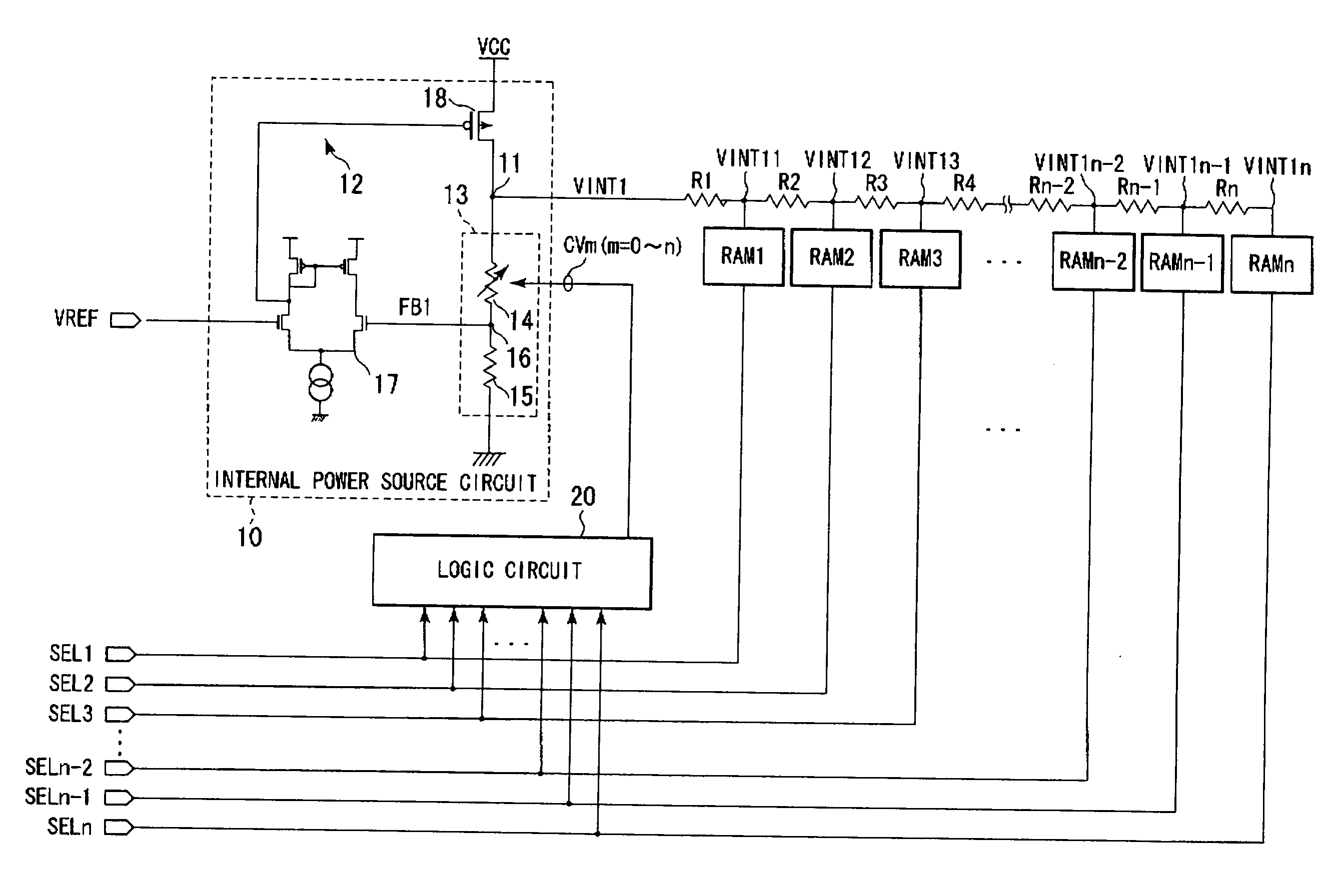
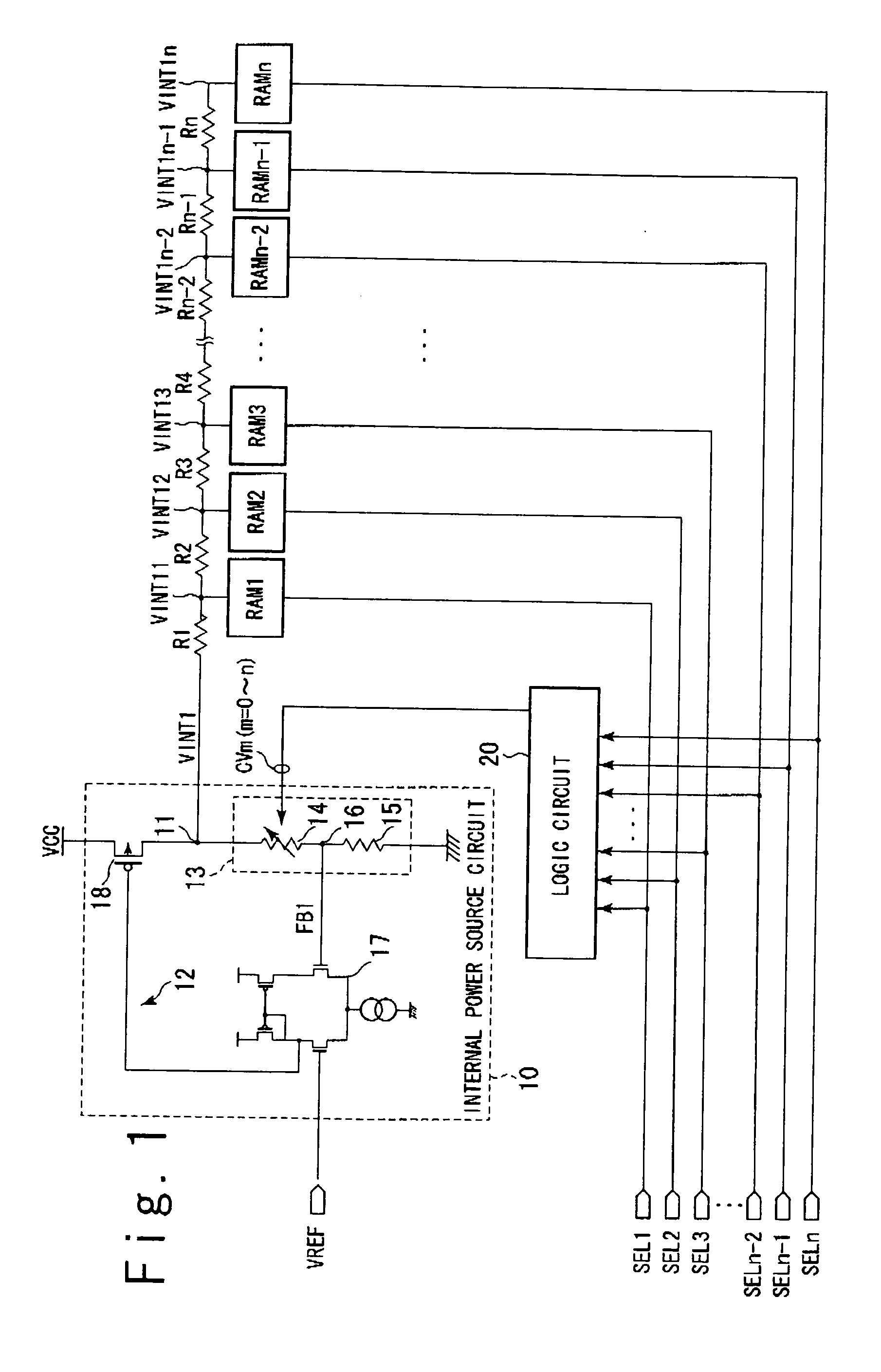
[0053]FIG. 1 is a view showing a configuration of the semiconductor integrated circuit device according to the first embodiment of the present invention. The semiconductor integrated circuit device includes a logic circuit 20, a high voltage driver circuit (not shown) for driving an LCD panel, an internal power source circuit 10 for generating an internal voltage, and a RAM (Random Access Memory) circuit. The RAM circuits transiently hold the pixel control information for controlling the LCD panel, using the internal voltage. The logic circuit 20, the high voltage driver circuit, the internal power source circuit 10 and the RAM circuit are arranged in the arrangement region of a chip.

[0054]The RAM circuit is divided into n number of RAM circuit blocks RAM1 to RAMn (n is an integer), as a plurality of RAM circuit blocks. These n number of the RAM circuit blocks RAM1 to RAMn are respectively connected to power source ports (which will be described later) different from ...

second embodiment

[0103]The first embodiment is described with regard to the case in which the number of the RAM circuit blocks currently in operation is one. However, the semiconductor integrated circuit device according to the second embodiment of the present invention is described with regard to the case in which a plurality of RAM circuit blocks currently in operation exist at the same time. In the second embodiment, the explanations overlapping with the first embodiment are omitted.

[Configuration]

[0104]The configuration of the semiconductor integrated circuit device according to the second embodiment of the present invention is similar to that of the first embodiment.

[Operation]

[0105]As an operation of the semiconductor integrated circuit device according to the second embodiment of the present invention, in order to simplify the description, a case is described in which two RAM circuit blocks currently in operation exist. Here, an operation current of one RAM circuit block is defined as Iact.

[0...

third embodiment

[0120]As the idea for falling in the ranges of the allowable internal power source voltage and the allowable access speed that is explained in the second embodiment, the semiconductor integrated circuit device according to the third embodiment of the present invention is described with regard to a method of decreasing an operation current of the RAM circuit block and decreasing the parasitic resistance of the internal power source wiring. In the third embodiment, the descriptions overlapping with those of the first and second embodiments are omitted.

[Configuration]

[0121]FIG. 12 is a view showing a configuration of the semiconductor integrated circuit device according to the third embodiment of the present invention. The RAM circuit in this semiconductor integrated circuit device is roughly divided into two portions and arranged, as the plurality of RAM circuit blocks. This RAM circuit is divided into: n number of RAM circuit blocks RAMR1 to RAMRn (n is the integer) in one group; and...


PUM


Abstract

A semiconductor integrated circuit device, includes: a RAM (Random Access Memory) circuit; and an internal power source circuit. The RAM circuit includes a plurality of RAM circuit blocks. The internal power source circuit supplies a voltage a selection RAM block selected from the plurality of RAM circuit blocks, wherein the voltage corresponds to an arrangement place of the selection RAM circuit block.

Description

INCORPORATED BY REFERENCE[0001]This application is based upon and claims the benefit of priority from Japanese patent application No. 2008-137606 filed on May 27, 2008, the disclosure of which is incorporated herein in its entirety by reference.BACKGROUND OF THE INVENTION[0002]1. Field of the Invention[0003]The present invention relates to a semiconductor integrated circuit device and more particularly relates to a semiconductor integrated circuit device having an internal voltage generating circuit, and a control method of the same.[0004]2. Description of Related Art[0005]As a semiconductor integrated circuit device, a liquid crystal display driver IC (hereafter, referred to as an LCD driver) is known for driving a liquid crystal display panel (hereafter, referred to as an LCD panel). The LCD driver is required to be arranged in the periphery of the LCD panel. For this reason, a chip of the LCD driver is required to have the long and thin shape in which an aspect ratio is unbalance...

Claims


Application Information

Patent Timeline
Patent Type & Authority Applications(United States)
IPC IPC(8): G09G5/00G11C5/14G09G3/36G11C8/00
CPCG11C5/147G11C5/063
Inventor OKAMOTO, TOSHIHARU
Owner RENESAS ELECTRONICS CORP
Learn More