Surface waveguide and method of manufacture

a surface waveguide and waveguide technology, applied in the field of optical waveguides, can solve the problems of increasing the magnitude of residual stress, increasing the induced strain, and many lpcvd-deposited thin films

Active Publication Date: 2005-08-18
OCTROLIX
View PDF11 Cites 38 Cited by
  • Summary
  • Abstract
  • Description
  • Claims
  • Application Information

AI Technical Summary

Benefits of technology

[0014] The conformal layer will fill the recess from the sidewalls inward. As a consequence, to fill a recess having a width that is equal to twice the critical thickness, the material need only deposit to a thickness that is equal to one times the critical thickness on each wall. The two layers, each having a thickness equal to the critical thickness, will meet along the centerline of the recess, completely filling it. Since it is acceptable to deposit material to a thickness up to and including the critical thickness, the material that is deposited within the recess will be of acceptable quality. If the recess is any wider than twice the critical thickness, the recess cannot be filled completely.

Problems solved by technology

Many LPCVD-deposited thin-films exhibit inherent residual stress and induced strain after deposition, primarily due to a mismatch of the coefficient of thermal expansion of the thin-film material and the substrate material.
The magnitude of residual stress can increase with film thickness, which leads to higher induced strain.
As a consequence of this behavior, there is a limit to the thickness to which many thin-film materials can be deposited.
Unfortunately, these materials are subject to the aforementioned critical-thickness constraint, thereby limiting their utility for use in surface waveguides.
In particular, thin films formed from stoichiometric silicon nitride are limited to a thickness of about 350 nm and thin films formed from TEOS have critical thickness limitation of about 1850 nm.

Method used


Image

  • Surface waveguide and method of manufacture
  • Surface waveguide and method of manufacture
  • Surface waveguide and method of manufacture

Examples


Embodiment Construction

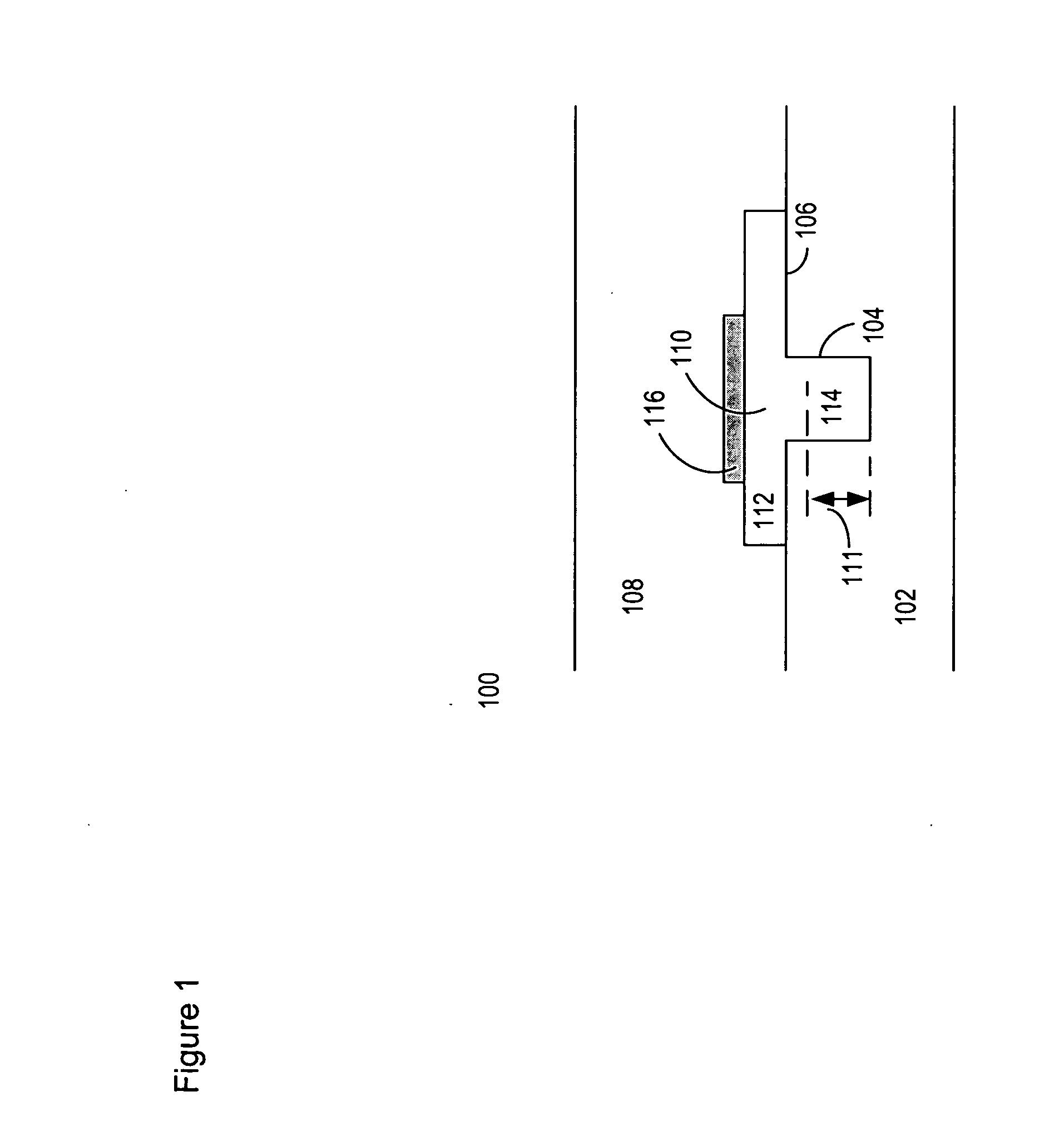
[0026]FIG. 1 depicts a cross-sectional view of a portion of inverted-ridge waveguide 100 in accordance with the illustrative embodiment of the present invention. Inverted-ridge waveguide 100 comprises core 110, lower cladding 102, and upper cladding 108.

[0027] Lower cladding 102 has a generally planar surface, with the exception of recess 104. The surface of lower cladding 102 on either side of recess 104 is referred to as “field region”106.

[0028] Core 110 comprises slab 112 and inverted ridge 114. The inverted ridge is disposed in recess 104. As described later in this specification, the width and height of inverted ridge 114 are determined by the width and depth of recess 104.

[0029] In the illustrative embodiment, inverted-ridge waveguide 100 includes optional layer 116 of electro-optically-active material. In some embodiments layer 116 is disposed on core 110. In such embodiments, layer 116 is functionally part of the core since it supports propagation of the optical signal. I...


PUM

PropertyMeasurementUnit
temperaturesaaaaaaaaaa
critical thicknessaaaaaaaaaa

Abstract

A surface waveguide is disclosed. In the illustrative embodiment, the waveguide has a core and an upper and lower cladding. The core has a thickness that is greater than the critical thickness of the material that composes the core. This is achieved by depositing/growing the core as a conformal layer within a region that is recessed from the planar surface of the lower cladding, wherein the recessed region has a width that is no more than twice the critical thickness of the core material.

Description

STATEMENT OF RELATED CASES [0001] This case claims priority of U.S. Provisional Patent Application No. 60 / 536,278, filed Jan. 13, 2004, and U.S. Provisional Patent Application No. 60 / 536,099, filed Jan. 13, 2004, both of which are incorporated herein by reference.FIELD OF THE INVENTION [0002] The present invention relates to optical waveguides in general, and, more particularly, to surface waveguides. BACKGROUND OF THE INVENTION [0003] A surface waveguide is a light-guiding element, much like an optical fiber, which is formed on the surface of a rigid substrate. Surface waveguides are used for many applications including telecommunications, chemical sensing, and force sensing. [0004] A surface waveguide is characterized as having a central region or “core” and a surrounding “cladding.” An optical signal travels through a surface waveguide as an optical mode propagating through the core. The optical signal is substantially confined to the core by the cladding. The guiding property of...

Claims


Application Information

Patent Timeline
Patent Type & Authority Applications(United States)
IPC IPC(8): G02B6/12G02B6/122G02B6/132
CPCG02B6/122G02B2006/121G02B2006/12097G02B6/132
Inventor HEIDEMAN, RENE GERRITHOEKMAN, MARCEL
Owner OCTROLIX
Why Eureka
Try Eureka