Exchange-coupled film, method for making exchange-coupled film, and magnetic sensing element including exchange-coupled film

a technology of exchange coupling and film, applied in the field of exchange coupling film, can solve the problems of not being able to form exchange coupling films, and achieve the effect of increasing the hex of the exchange coupling magnetic field and improving the wettability of the surface of the seed layer

Inactive Publication Date:
View PDF36 Cites 25 Cited by
  • Summary
  • Abstract
  • Description
  • Claims
  • Application Information

AI Technical Summary

Benefits of technology

[0072] Additionally, as in the present invention, when the surface of the seed layer is etched, the Cr concentration at the outermost surface of the finished seed layer may be slightly lower than the Cr concentration inside the seed layer and the Ni concentration at the outermost surface of the finished seed layer may be slightly higher than the Ni concentration inside the seed layer. If such a concentration gradient occurs, it is believed that the surface energy of the seed layer changes, and the wettability of the surface of the seed layer improves, resulting in an increase in the exchange coupling magnetic field Hex between the antiferromagnetic layer and the ferromagnetic layer. This concentration gradient is caused by the step of etching the surface of the seed layer and does not occur in the conventional seed layer.

Problems solved by technology

As described above, because the seed layer has the critical thickness below which the change in resistance ΔRs and the rate of change in resistance ΔRs / Rs rapidly decrease, it has not been possible to form an exchange-coupled film in which the thickness of the seed layer is smaller than or equal to the critical thickness or a magnetic sensing element including such an exchange-coupled film.

Method used


Image

  • Exchange-coupled film, method for making exchange-coupled film, and magnetic sensing element including exchange-coupled film
  • Exchange-coupled film, method for making exchange-coupled film, and magnetic sensing element including exchange-coupled film
  • Exchange-coupled film, method for making exchange-coupled film, and magnetic sensing element including exchange-coupled film

Examples


examples

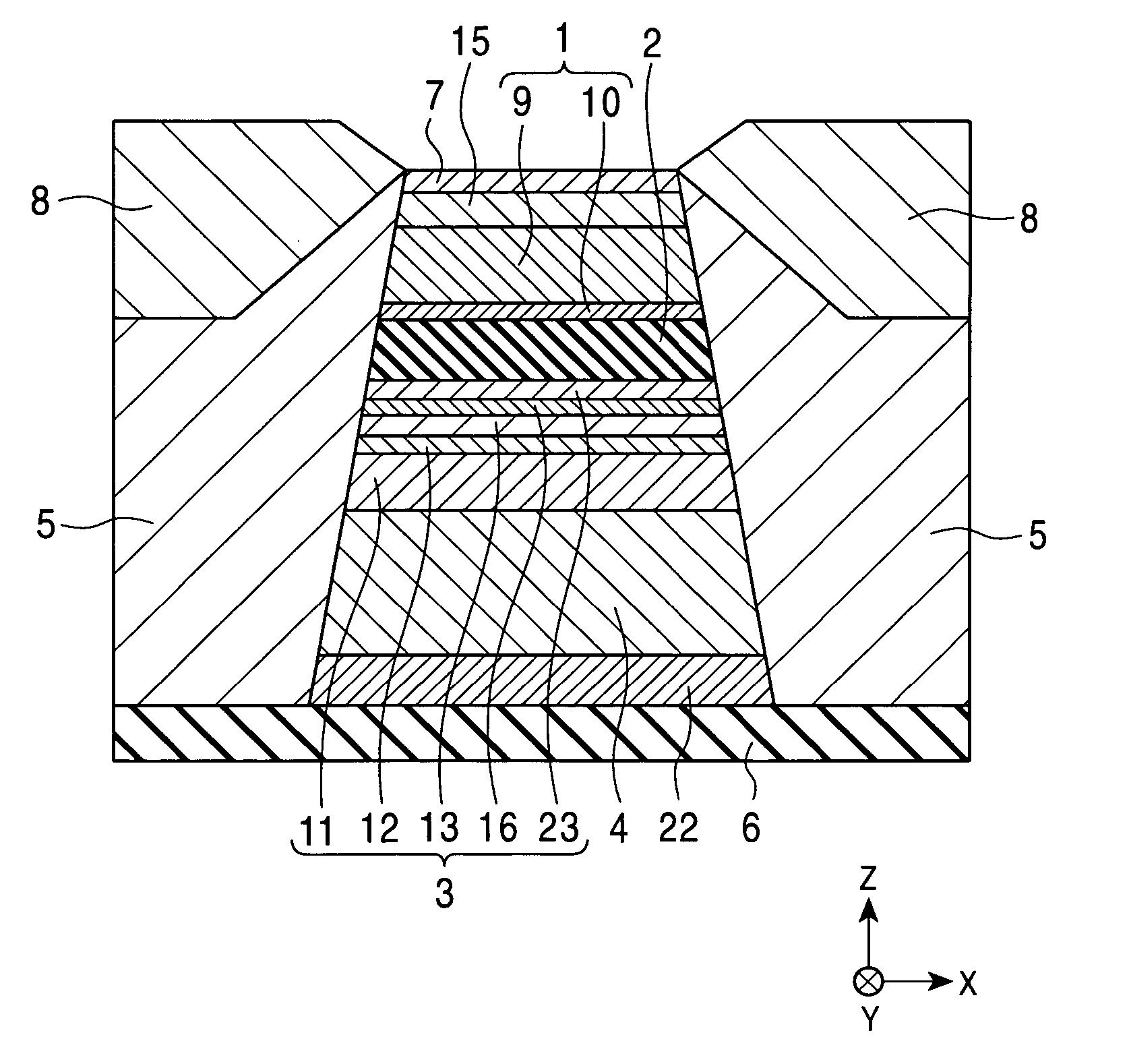
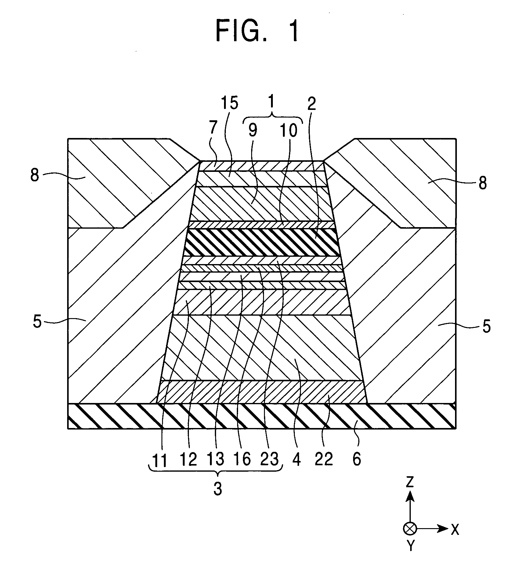
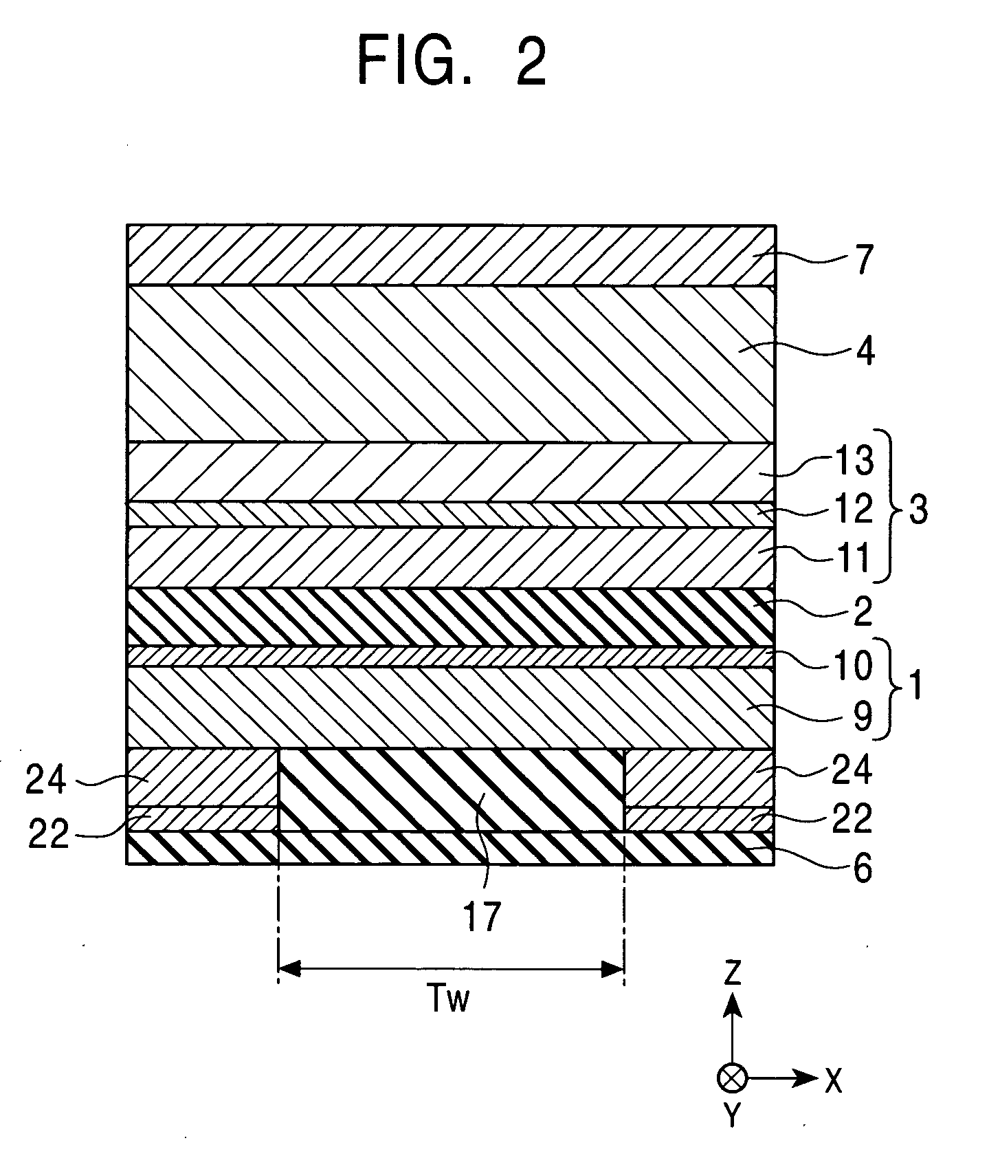
[0262] Magnetic sensing elements were fabricated for testing. In order to fabricate each magnetic sensing element, a seed layer was formed using a (Ni0.8Fe0.2)60Cr40 alloy at a thickness of 42 Å by sputtering, and the upper surface of the seed layer was etched so that the thickness of the seed layer was smaller than or equal to the critical thickness, i.e., 38 Å. Plasma etching (inverse sputtering) or ion beam etching was used to etch the seed layer. Furthermore, a structure of antiferromagnetic layer [PtMn (140 Å)] / pinned magnetic layer [CoFe (16 Å) / Ru (8.7 Å) / CoFe (22 Å)] / nonmagnetic layer [Cu (19 Å)] / free magnetic layer [CoFe (10 Å) / NiFe (35 Å)] / protective layer [Ta (30 Å)] was continuously formed by sputtering on the seed layer.

[0263] By changing the amount removed from the seed layer, magnetic sensing elements having seed layers with different thicknesses were prepared. The rate of change in resistance ΔRs / Rs, the change in resistance ΔRs, the sheet resistance Rs, and the unid...


PUM

PropertyMeasurementUnit
sheet resistance Rsaaaaaaaaaa

Abstract

An exchange-coupled film includes a seed layer, an antiferromagnetic layer, and a ferromagnetic layer. The seed layer is formed at a thickness that is larger than the critical thickness, and the thickness of the seed layer is then decreased by etching so as to be smaller than or equal to the critical thickness. Thereby, a crystalline phase which extends through the seed layer from the upper surface to the lower surface can be formed, and/or the average size, in a direction parallel to the layer surface, of the crystal grains in the seed layer can be set to be larger than the thickness of the seed layer. Consequently, a large exchange coupling magnetic field Hex can be generated between the antiferromagnetic layer and the ferromagnetic layer.

Description

BACKGROUND OF THE INVENTION [0001] 1. Field of the Invention [0002] The present invention relates to an exchange-coupled film which includes a seed layer, an antiferromagnetic layer, and a ferromagnetic layer disposed in that order from the bottom and in which the magnetization direction of the ferromagnetic layer is pinned in a predetermined direction by an exchange coupling magnetic field generated at the interface between the antiferromagnetic layer and the ferromagnetic layer; a method for making the exchange-coupled film; and a magnetic sensing element including the exchange-coupled film. More particularly, the invention relates to an exchange-coupled film in which the total thickness and shunt loss can be decreased by decreasing the thickness of the seed layer thereof, a method for making the exchange-coupled film, and a magnetic sensing element including the exchange-coupled film. [0003] 2. Description of the Related Art [0004]FIG. 27 is a partial sectional view of a conventi...

Claims


Application Information

Patent Timeline
Patent Type & Authority Applications(United States)
IPC IPC(8): G01R33/09G11B5/39H01F10/30H01F10/32H01F41/14H01F41/30H01L43/08H01L43/12
CPCH01F41/308B82Y25/00B82Y40/00G01R33/093G11B5/3906H01F41/325H01F10/30H01F10/3263H01F10/3272Y10T29/49032Y10T29/49021G11B5/3932
Inventor NAKABAYASHI, RYOUUMETSU, EIJIHASEGAWA, NAOYA
Why Eureka
Try Eureka