Strained silicon on a SiGe on SOI substrate

a technology of strained silicon and substrate, which is applied in the direction of semiconductor devices, electrical apparatus, transistors, etc., can solve the problems of limiting the concentration of germanium in sige-on-insulator substrates, the current method of forming strained silicon on soi suffers drawbacks, and the procedure is relatively expensiv

Active Publication Date: 2005-05-19
GLOBALFOUNDRIES US INC
View PDF90 Cites 24 Cited by
  • Summary
  • Abstract
  • Description
  • Claims
  • Application Information

AI Technical Summary

Benefits of technology

[0011] In a third aspect of the invention, an intermediate semiconductor structure is formed on a substrate. The structure includes a semiconductor substrate and a relaxed Si1-xGex portion on a semiconductor substrate. The relaxed Si1-xGex portion inc

Problems solved by technology

Unfortunately, however, current methods for forming strained silicon on SOI suffer drawbacks.
A problem with SIMOX is that it is relatively costly procedure.
Another problem is that the high SIMOX annealing temperature (1350° C.) limits the concent

Method used


Image

  • Strained silicon on a SiGe on SOI substrate
  • Strained silicon on a SiGe on SOI substrate
  • Strained silicon on a SiGe on SOI substrate

Examples


Embodiment Construction

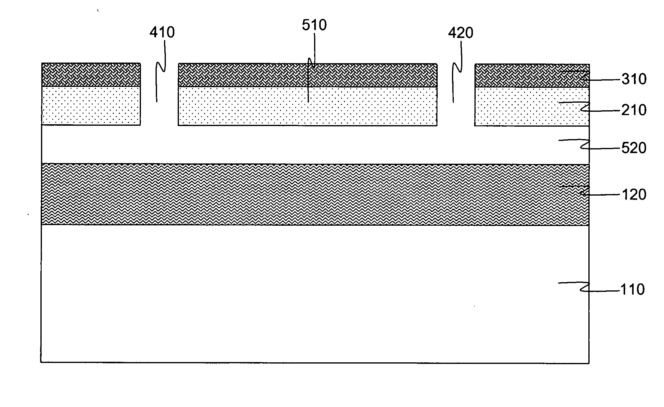
[0025] The invention enables fabrication of a strained silicon layer on a SiGe-on-insulator substrate. An exemplary methodology in accordance with the invention entails undercutting a SiGe layer to form a relaxed SiGe island, filling the voids with a dielectric and epitaxially growing Si on the relaxed SiGe. The strained Si thus formed can be free of dislocations and misfits. The resulting structure can also be fabricated cost effectively using conventional processing equipment and materials. Additionally, the structure allows a thin SiGe layer, which enables shallow junctions and enhanced device performance.

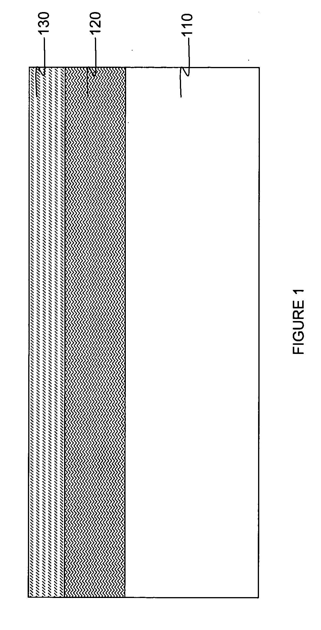
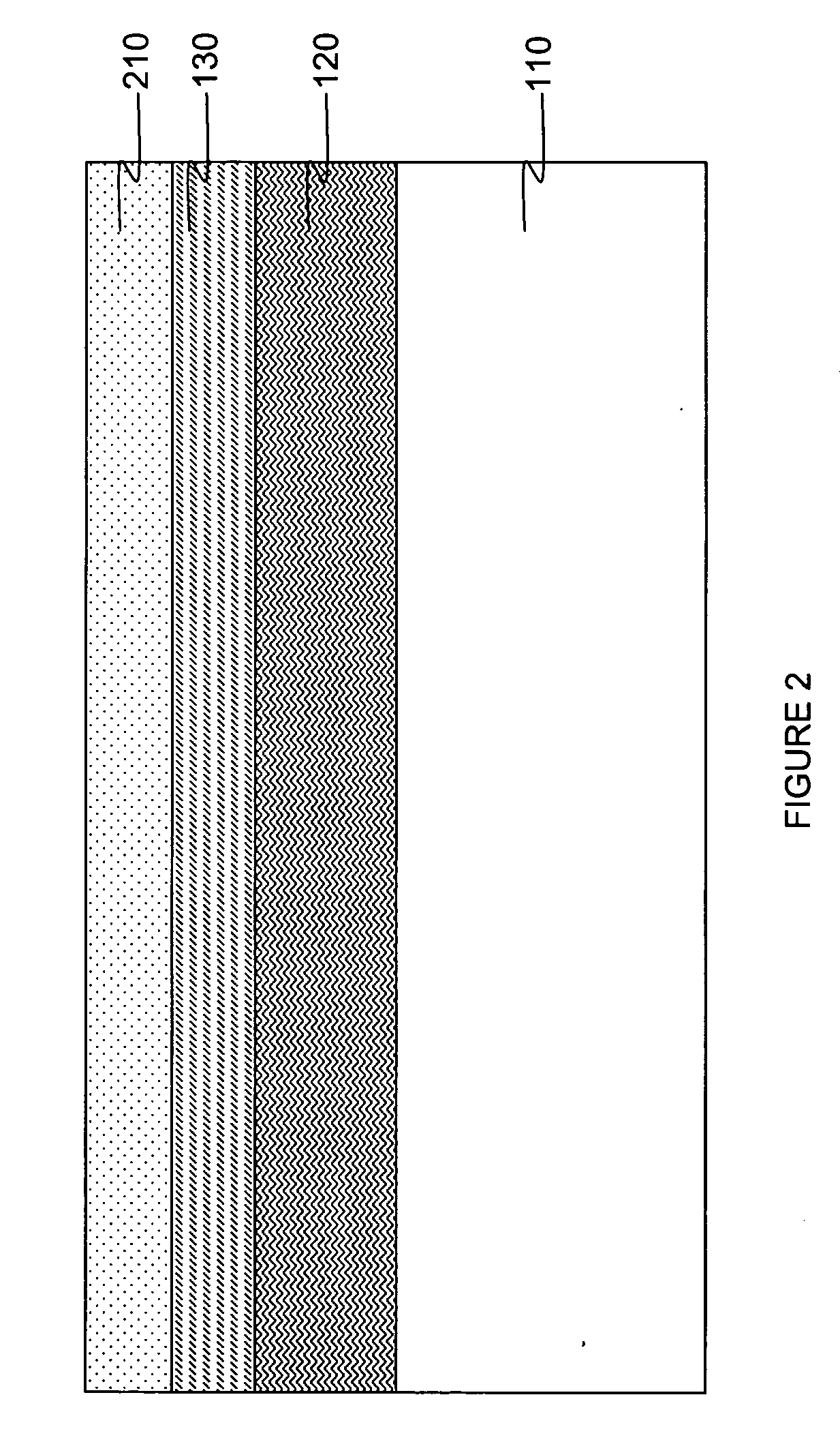
[0026] Referring now to FIG. 1, a silicon-on-insulator (SOI) wafer is shown. Such wafers are commercially available starting substrates for various discrete and integrated circuit (IC) semiconductor device applications. The wafer includes a buried silicon oxide (BOX) layer 120 extending across the entire wafer, just below a thin (e.g., 5 to 200 nm) surface layer of device-quali...


PUM


Abstract

A semiconductor device with an undercut relaxed SiGe layer having voids beneath the SiGe layer. The voids may be filled with a dielectric such as SiO2. A strained Si layer may be epitaxially grown on the relaxed SiGe layer to combine the benefits of a defect-free strained Si surface and a silicon-on-insulator substrate. The relaxed SiGe layer may be relatively thin, with a thickness below the critical thickness. Thus, the structure accommodates shallow junctions, which exhibit reduced junction capacitance.

Description

BACKGROUND OF THE INVENTION [0001] 1. Field of the Invention [0002] The invention generally relates to a semiconductor device and method of manufacture and, more particularly, to a semiconductor device that includes strained silicon on a SiGe on a silicon-on-insulator substrate. [0003] 2. Background Description [0004] Various techniques have emerged to improve performance of state of the art semiconductors. One technique involves introducing strain. Strained silicon exhibits improved semiconductor performance due to enhanced transport properties. Biaxial distortion of the crystal lattice in strained silicon improves electron and hole mobility. [0005] Another performance enhancement technique involves providing a semiconductor layer separated from the substrate by an insulating layer. Also known as silicon-on-insulator (SOI), such structures exhibit reduced parasitic capacitance, thereby enabling a semiconductor to function at significantly higher speeds with reduced electrical losse...

Claims


Application Information

Patent Timeline
IPC IPC(8): H01L21/20H01L21/336H01L21/762H01L29/10H01L29/786
CPCH01L21/02381H01L21/02532H01L21/02658H01L21/2007Y10S438/933H01L29/1054H01L29/66742H01L29/78603H01L29/78687H01L21/76251
Inventor CHENG, KANGGUOCHIDAMBARRAO, DURESETI
Owner GLOBALFOUNDRIES US INC
Why Eureka
Try Eureka