Clock duty ratio correction circuit

Active Publication Date: 2005-08-25
SK HYNIX INC
View PDF5 Cites 33 Cited by
  • Summary
  • Abstract
  • Description
  • Claims
  • Application Information

AI Technical Summary

Benefits of technology

[0012] Accordingly, it is an object of the present invention to providing an improved clock duty ratio correction circuit for correcting a duty ratio of high resolution wit

Problems solved by technology

However, the method of controlling the size of MOS transistors has degraded correction resolution, and its use is improper in a system for receiving a differential clo

Method used


Image

  • Clock duty ratio correction circuit
  • Clock duty ratio correction circuit
  • Clock duty ratio correction circuit

Examples


Example

[0024] The present invention will be described in detail with reference to the accompanying drawings.

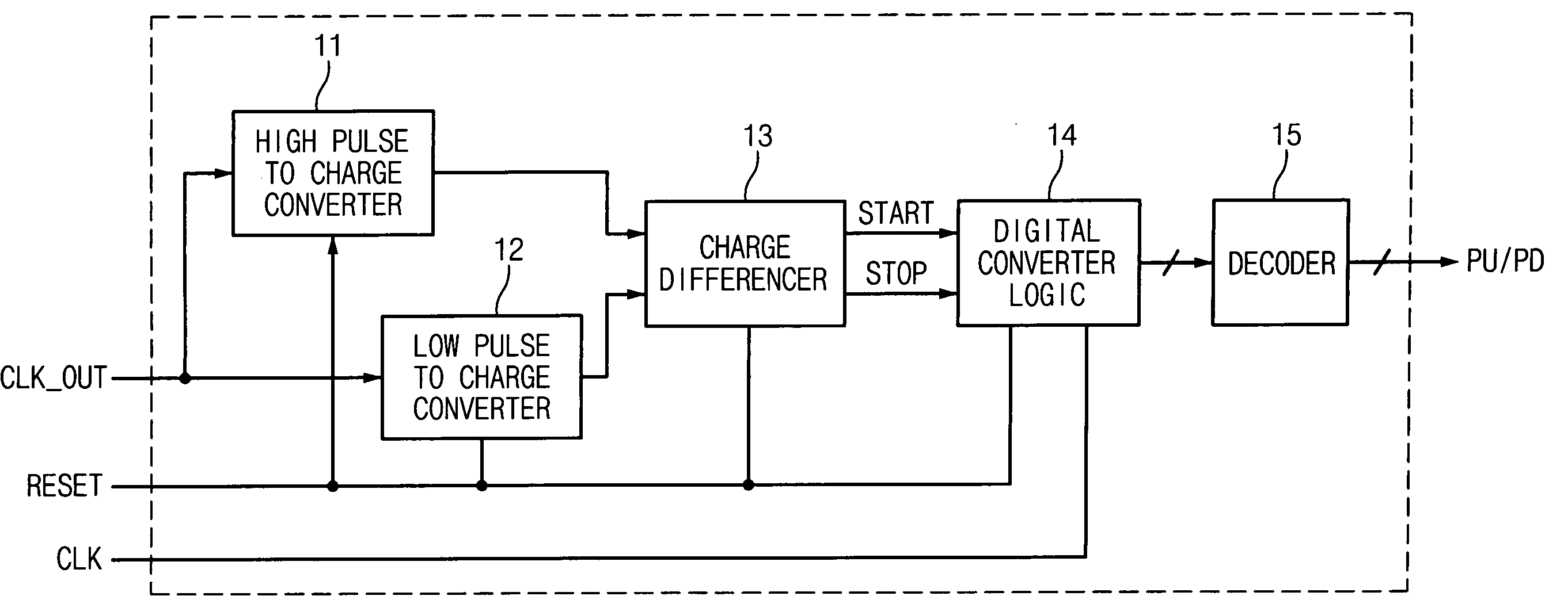
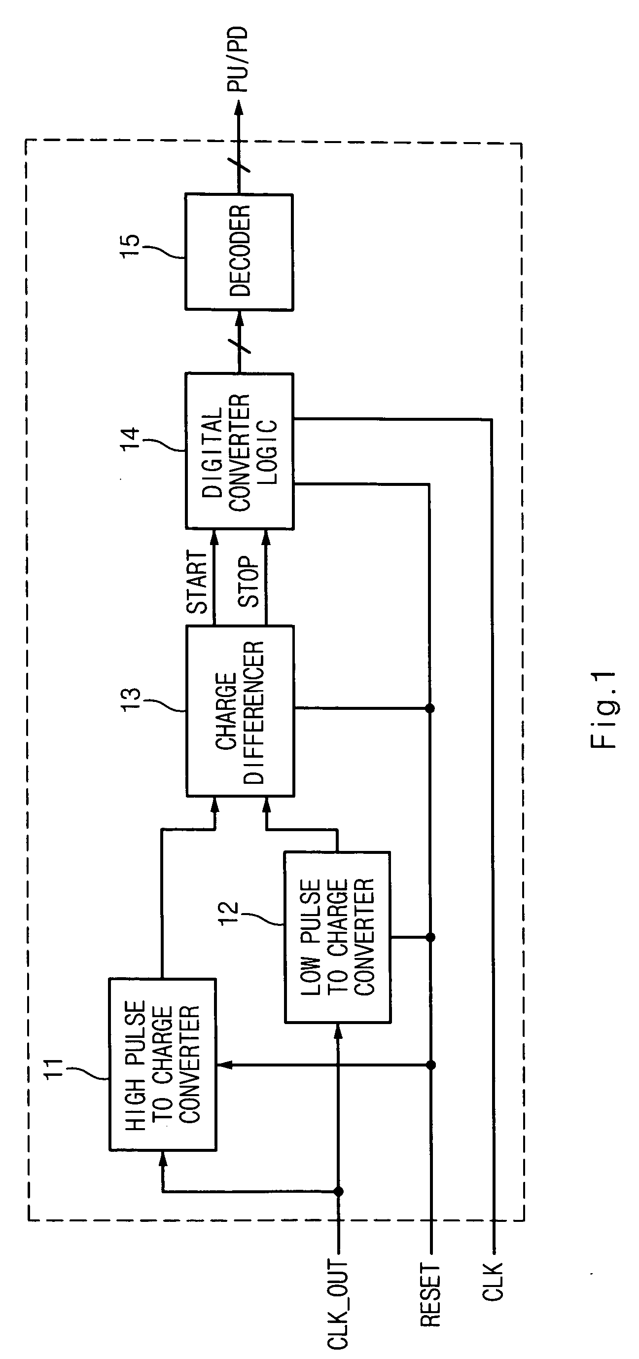
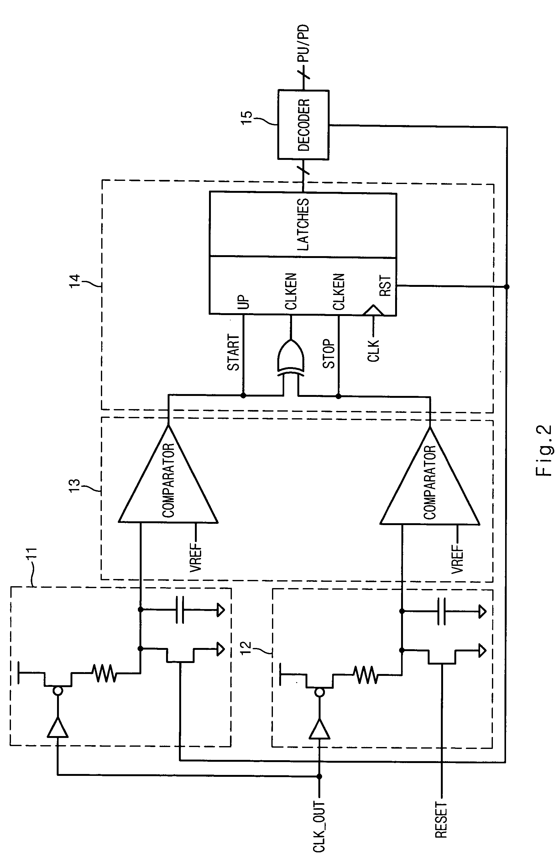
[0025]FIG. 3 is a block diagram of a clock duty ratio correction circuit according to an embodiment of the present invention.

[0026] In an embodiment, the clock duty ratio correction circuit comprises a rising clock buffer 100, a falling clock buffer 200, a charge pump unit 300, a comparison control unit 400, a voltage comparison unit 500, a counter 600 and a D / A converter 700.

[0027] The rising clock buffer 100 and the falling clock buffer 200 correct differential internal clock signals iRCLK and iFCLK to have a duty ratio of 1:1 depending on voltage levels of duty ratio correcting signals RVREF / FVREF applied from the D / A converter 700 regardless of the duty ratio of differential clock signals CLK and CLKB inputted externally. Then, the clock buffers 100 and 200 change a logic threshold of a NMOS transistor connected serially to a NMOS transistor for receiving the differential cloc...


PUM


Abstract

A clock duty ratio correction circuit corrects a duty ratio of internal clock signals at 1:1. The clock duty ratio correction circuit comprises a clock buffer unit, a charge pump unit, a comparison control unit, a voltage comparison unit, a counter and a D/A converter. The clock duty ratio correction circuit converts a differential internal clock signal into a voltage level corresponding to the pulse width of the differential internal clock signal, and compares the voltage level to generate a count signal. Additionally, the clock duty ratio correction circuit divides a reference voltage at a predetermined ratio in response to the count signal to generate a duty ratio correcting signal, and corrects the duty ratio of the differential internal clock signal by using the voltage level difference of the duty ratio correcting signal.

Description

BACKGROUND OF THE INVENTION [0001] 1. Field of the Invention [0002] The present invention generally relates to a clock duty ratio correction circuit for maintaining a clock signal to have a duty ratio of 1:1, and more specifically, to a clock duty ratio correction circuit for electrically converting an internal clock signal and then generating the internal clock signal having a predetermined duty ratio of 1:1 regardless of an externally applied clock signal by using a level difference of the converted electrical signal. [0003] 2. Description of the Prior Art [0004] It is important to precisely control a duty ratio of a clock signal in a semiconductor device for inputting / outputting data by using the clock signal. [0005] In generally, a clock signal having a duty ratio of 50% has been widely used in a digital clock application field such as a semiconductor integrated circuit. The 50% duty ratio means that a high level of the clock signal is the same as a low level of the clock signal...

Claims


Application Information

Patent Timeline
IPC IPC(8): H03K3/017H03L5/00H03K5/156
CPCH03K5/1565H03L5/00
Inventor CHUN, JUN HYUN
Owner SK HYNIX INC
Why Eureka
Try Eureka