Capacitor bank and voltage controlled oscillator having the same

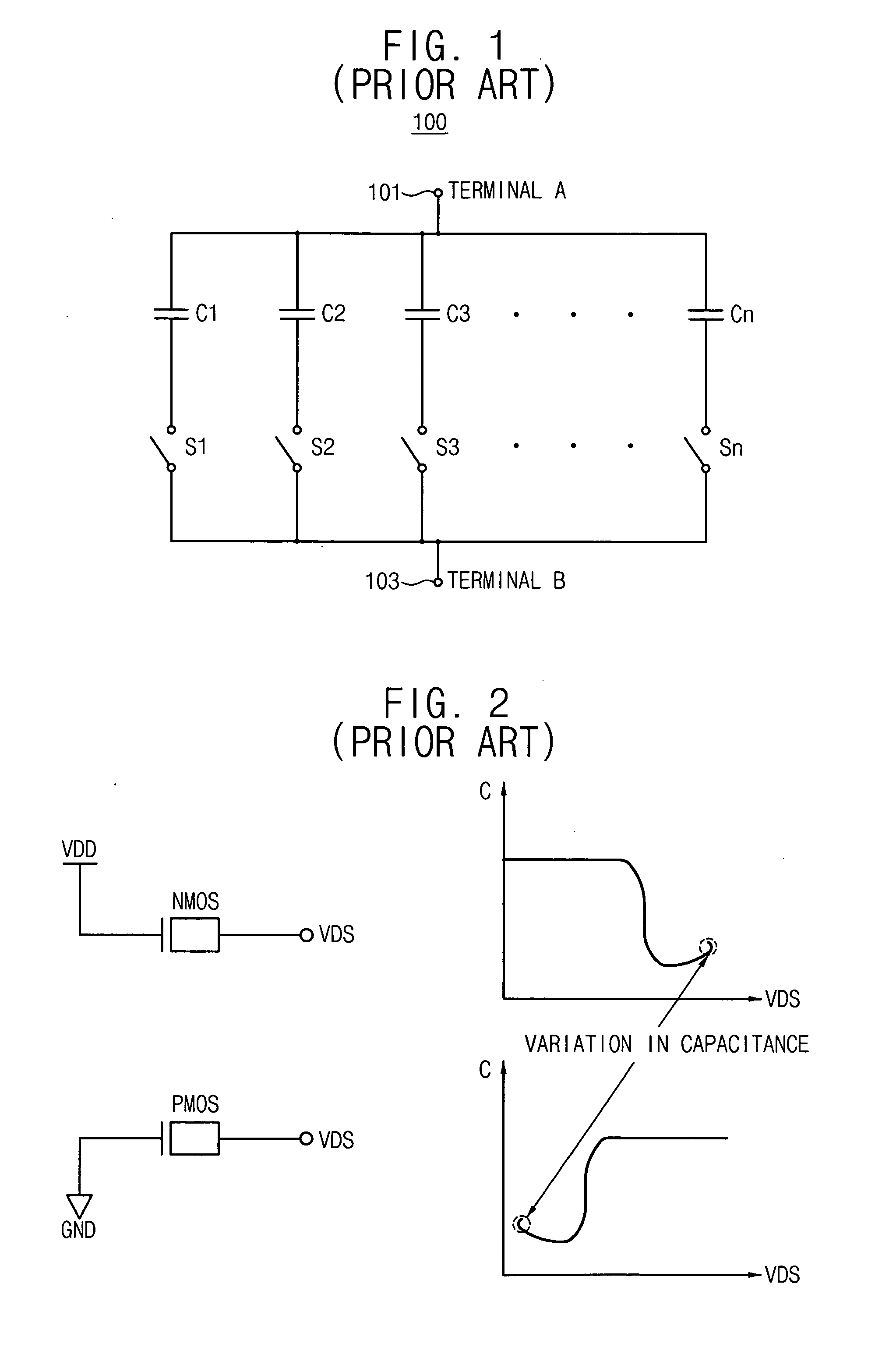
a voltage-controlled oscillator and capacitor bank technology, applied in oscillation generators, angle modulation details, resonance circuit tuning, etc., can solve the problems of phase noise degradation due to fm modulation, the capacitor bank of fig. 1 may not be used in the voltage-controlled oscillator, and the difficulty in achieving high quality factor (q)

Active Publication Date: 2005-08-25
SAMSUNG ELECTRONICS CO LTD
View PDF6 Cites 51 Cited by
  • Summary
  • Abstract
  • Description
  • Claims
  • Application Information

AI Technical Summary

Benefits of technology

[0018] Exemplary embodiments of the present invention provide a capacitor bank to prevent the phase noise degradation due to FM modulation when the common noise is introduced to the DC voltage of the oscillation node.

Problems solved by technology

However, a high quality factor (Q) is difficult to achieve in the capacitor bank of FIG. 1 because of the on-resistance of switches S1 to Sn that are serially connected to the MIM capacitors C1 to Cn.
That is, when the voltage-controlled oscillator is designed for low noise and wide bandwidth environment, the MIM capacitor bank may not be used in the voltage-controlled oscillator.
Therefore, when common noise is introduced into the DC voltage at the terminal A 501 or terminal B of the capacitor bank, phase noise degradation due to FM modulation may occur.

Method used


Image

  • Capacitor bank and voltage controlled oscillator having the same
  • Capacitor bank and voltage controlled oscillator having the same
  • Capacitor bank and voltage controlled oscillator having the same

Examples


Embodiment Construction

[0032] The present invention will become more apparent to those of ordinary skill in the art by describing, in detail, exemplary embodiments thereof with reference to the attached drawings, wherein like elements are represented by like reference numerals, which are given by way of illustration only and thus do not limit the exemplary embodiments of the present invention.

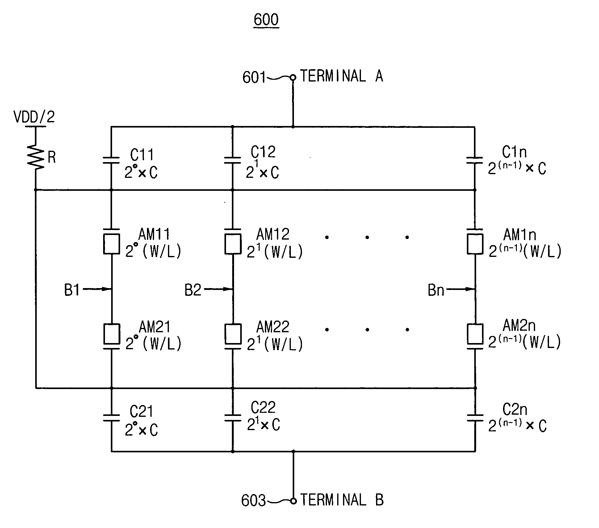
[0033]FIG. 6 is a circuit diagram illustrating a capacitor bank in a differential mode using blocking capacitors and AMOS varactors according to an exemplary embodiment of the present invention.

[0034] Referring to FIG. 6, the capacitor bank 600 has a terminal A 601, a terminal B 603, first blocking capacitors C11 to C1n, first AMOS varactors AM11 to AM1n, second blocking capacitors C21 to C2n and second AMOS varactors AM21 to AM2n.

[0035] The first blocking capacitors C11 to C1n have first terminals commonly connected to the terminal A 601 and second terminals to which a bias voltage (VDD / 2) is applied. The first A...


PUM


Abstract

A capacitor bank includes a first node, a second node, first blocking capacitors, N first AMOS varactors, second blocking capacitors and N second AMOS varactors. The first blocking capacitors have first terminals connected to the first node and second terminals where a bias voltage is applied. The N first AMOS varactors have first terminals connected to the second terminals of the first block capacitors. The second blocking capacitors have first terminals connected to the second node and second terminals where the bias voltage is applied. The N second AMOS varactors have first terminals connected to the second terminals of the second blocking capacitors and second terminals connected to second terminals of the first AMOS varactors, respectively, wherein N binary coded signals are applied to the respective second terminals of the first AMOS varactors and the second AMOS varactors. Therefore, phase-noise degradation caused by the FM modulation may be avoided.

Description

CROSS-REFERENCE TO RELATED APPLICATION [0001] This application claims priority under 35 USC § 119 to Korean Patent Application No. 2004-11239, filed on Feb. 20, 2004 in the Korean Intellectual Property Office, the disclosure of which is incorporated by reference herein in its entirety. BACKGROUND OF THE INVENTION [0002] 1. Field of the Invention [0003] The present invention relates to a capacity bank and a voltage-controlled oscillator having the same, capable of preventing phase noise degradation due to the FM modulation when common noise is introduced into the DC voltage of an oscillation node of the capacitor bank. [0004] 2. Description of the Related Art [0005] As communication systems become increasingly complex, each single chip for a transceiver is generally designed with a voltage-controlled oscillator (VCO) that supports both multi-band communication and the use of multi-mode. A transceiver integrated circuit (IC) for mobile communication requires the VCO to operate over a ...

Claims


Application Information

Patent Timeline
Patent Type & Authority Applications(United States)
IPC IPC(8): H03B1/00H03B5/12H03L7/00
CPCH03B2201/025H03B5/1215H03B5/1228H03J2200/10H03B5/12
Inventor CHO, JE-KWANG
Owner SAMSUNG ELECTRONICS CO LTD
Why Eureka
Try Eureka