Organic light emitting display device and method of manufacturing the same

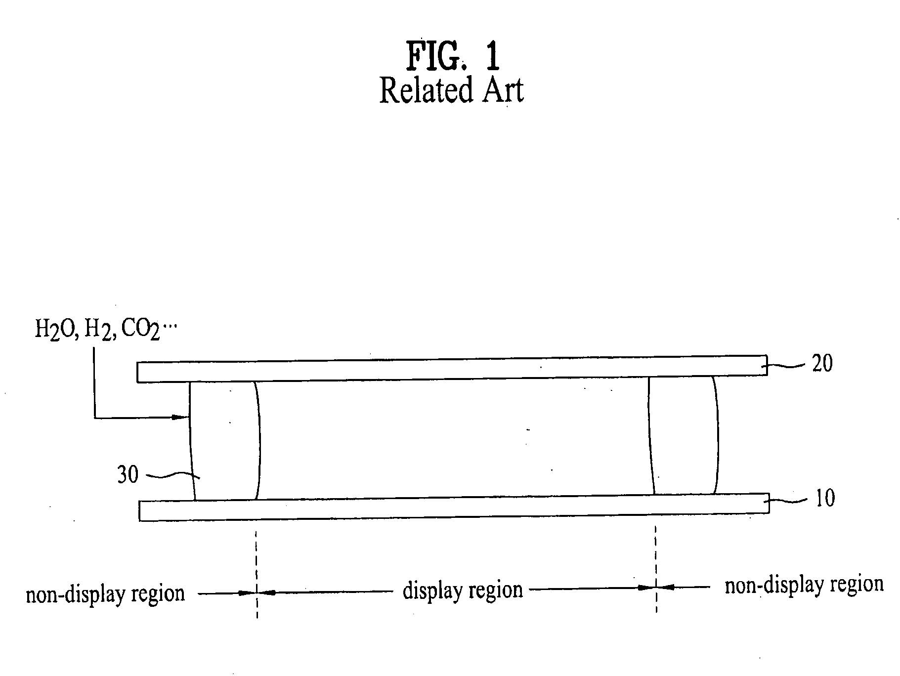
a technology of light-emitting display and organic light-emitting tubes, which is applied in the manufacture of electrode systems, electric discharge tubes/lamps, discharge tubes luminescnet screens, etc., and can solve the problems of increasing the severity of the hygroscopic phenomenon, many restrictions on the resolution of the passive matrix type structure, and limited use of hygroscopic agents

Active Publication Date: 2008-12-04
LG DISPLAY CO LTD
View PDF7 Cites 59 Cited by
  • Summary
  • Abstract
  • Description
  • Claims
  • Application Information

AI Technical Summary

Benefits of technology

[0024]To achieve these objects and other advantages and in accordance with the purpose 6f the invention, as embodied and broadly described herein, an organic light emitting display device includes a first substrate and a second substrate being opposite to each other, the first substrate and the second substrate having a display region defined in the middle thereof and a non-display region defined at the edge thereof, respectively, a plurality of gate lines and data lines formed at the display region on the first substrate, the gate lines and the data lines crossing each other to define a pixel region, a thin film transistor formed at each of the intersections between the gate lines and data lines, an organic light emitting layer formed on the second substrate corresponding to the pixel region, and first and second electrodes located above and below the organic light emitting layer and a sealing structure connected between the first and second substrates, such that the first and second substrates are bonded to each other by the sealing structure, for preventing the permeation of moisture and gas.

Problems solved by technology

However, the passive matrix type structure is under many restrictions relating to resolution, power consumption, and service life.
Furthermore, the use of the hygroscopic agent is limited to fundamentally prevent the permeation of moisture.
Also, the hygroscopic phenomenon becomes more serious with the passage of time, and the shrinkage phenomenon of the respective pixels located inside the seal pattern 30 becomes more serious.
As a result, the service life of the organic light emitting display device under the hygroscopic phenomenon decreases.
The ultraviolet curing type organic seal pattern has problems in that moisture or the like may easily permeate into the seal pattern according to external environment, and the seal pattern may be easily separated from the substrates, which are made of glass, whereby external gases are introduced into the display region to degrade the organic light emitting layer from the edge of the organic light emitting layer, with the result that the size of the pixels decreases.
There are many restrictions in solving such degradation problem, and therefore, there is a high necessity to improve a material for the seal pattern.

Method used


Image

  • Organic light emitting display device and method of manufacturing the same
  • Organic light emitting display device and method of manufacturing the same
  • Organic light emitting display device and method of manufacturing the same

Examples


first embodiment

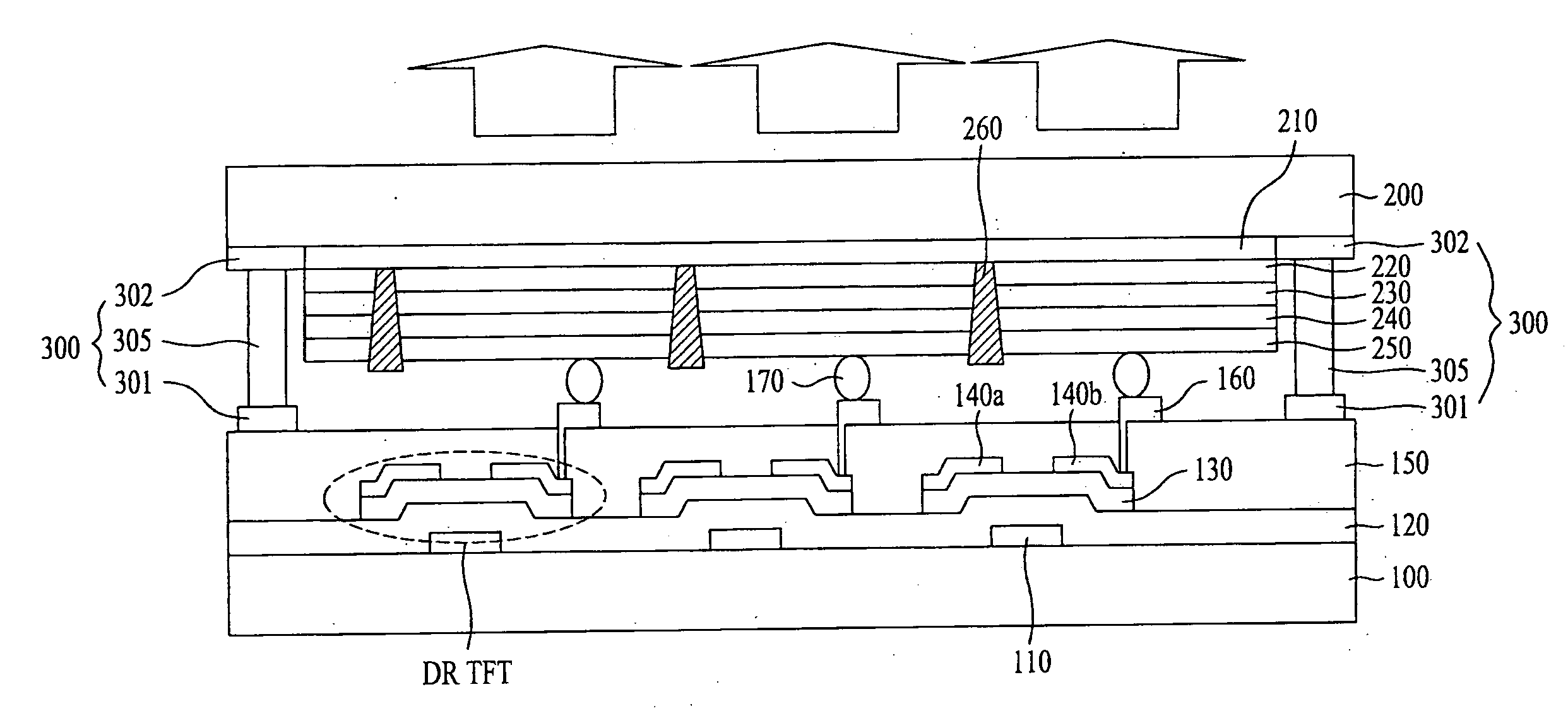
[0059]FIG. 3 is a sectional view illustrating a sealing structure of an organic light emitting display device according to the present invention, and FIG. 4 is a plan view schematically illustrating the organic light emitting display device of FIG. 3.

[0060]As shown in FIGS. 3 and 4, the sealing structure of the organic light emitting display device according to the first embodiment of the present invention includes a first substrate 100 having a display region (within a dotted-line region of FIG. 4) defined in the middle thereof and a non-display region defined at the edge thereof, a second substrate 200 having a display region defined in the middle thereof and a non-display region defined at the edge thereof, the first substrate 100 and the second substrate 200 being opposite to each other, and a seal unit 300 formed between first substrate 100 and the second substrate 200 at positions corresponding to the non-display regions.

[0061]The seal unit 300 includes a first metal oxide fil...

second embodiment

[0069]FIGS. 5A and 5B are sectional views respectively illustrating sealing structures of an organic light emitting display device according to the present invention and a modification thereof, and FIG. 6 is a plan view illustrating the organic light emitting display device of FIGS. 5A and 5B.

[0070]As shown in FIGS. 5A and 6, the organic light emitting display device according to the second embodiment of the present invention is similar in structure to the organic light emitting display device according to the first embodiment of the present invention in that a seal unit 310 includes first and second metal oxide films 311 and 312 and a connection electrode pattern 315 for interconnecting the first and second metal oxide films 311 and 312. However, the organic light emitting display device according to the second embodiment of the present invention is different in structure from the organic light emitting display device according to the first embodiment of the present invention in th...

third embodiment

[0076]FIGS. 7A and 7B are sectional views illustrating sealing structures of an organic light emitting display device according to the present invention, and FIG. 8 is a plan view illustrating the organic light emitting display device including areas corresponding to FIGS. 7A and 7B.

[0077]As shown in FIG. 8, the organic light emitting display device according to the third embodiment of the present invention includes a seal pattern 350 made of an ultraviolet curing type organic material and a seal unit 360 made of a metal compound. The seal pattern 350 and the seal unit 360 are located at a non-display region.

[0078]Here, the seal pattern 350 is formed in the shape of a frame surrounding the edge of a display region. The seal unit 360 is formed in the shape of a frame spaced a predetermined distance from the seal pattern 350 such that the frame of the seal unit 360 is located outside the frame of the seal pattern 350 along the edge of the second substrate 200.

[0079]Here, the seal unit...


PUM


Abstract

An organic light emitting display device that is capable of preventing the permeation of moisture by changing a sealing structure, thereby preventing the degradation of pixels and thus improving look-and-feel characteristics and a method of manufacturing the same are disclosed. The organic light emitting display device includes a first substrate and a second substrate being opposite to each other, the first substrate and the second substrate having a display region defined in the middle thereof and a non-display region defined at the edge thereof, respectively, a plurality of gate lines and data lines formed at the display region on the first substrate, the gate lines and the data lines crossing each other to define a pixel region, a thin film transistor formed at each of the intersections between the gate lines and data lines, an organic light emitting layer formed on the second substrate corresponding to the pixel region, and first and second electrodes located above and below the organic light emitting layer and a sealing structure connected between the first and second substrates, such that the first and second substrates are bonded to each other by the sealing structure, for preventing the permeation of moisture and gas.

Description

CROSS-REFERENCE TO RELATED APPLICATION[0001]This application claims the benefit of Korean Patent Application No. P 2007-0053108, filed on May 30, 2007 and No. P 2007-067379, filed on Jul. 5, 2007, which are hereby incorporated by reference in its.BACKGROUND OF THE INVENTION[0002]1. Field of the Invention[0003]The present invention relates to an organic light emitting display device, and more particularly, to an organic light emitting display device that is capable of preventing the permeation of moisture by changing a sealing structure and a material, thereby preventing the degradation of pixels and thus improving look-and-feel characteristics and a method of manufacturing the same.[0004]2. Discussion of the Related Art[0005]An organic light emitting display device, one of the flat panel displays, is a self-luminous type display device. Consequently, the organic light emitting display device has a higher contrast than a liquid crystal display. Also, the organic light emitting displa...

Claims


Application Information

Patent Timeline
Patent Type & Authority Applications(United States)
IPC IPC(8): H01J1/63H01J9/26
CPCH01L27/3251H01L51/5237H10K59/127H10K50/8423H10K50/8428H10K50/8426H10K50/844
Inventor AHN, BYUNG CHULPARK, JAE YONGKIM, KYUNG MANKIMLEE, KANG JUKIM, HO JIN
Owner LG DISPLAY CO LTD
Why Eureka
Try Eureka