Semiconductor storage device

a technology of semiconductors and storage devices, applied in the direction of transistors, solid-state devices, instruments, etc., can solve the problems of increasing the difficulty of conventional 1t-1c (one transistor-one capacitor) type dram cells to be manufactured, the inability of conventional fbc cells to employ an open bit line structure, and the difficulty in the layout of sense amplifiers

Inactive Publication Date: 2005-09-01
KK TOSHIBA
View PDF7 Cites 107 Cited by
  • Summary
  • Abstract
  • Description
  • Claims
  • Application Information

AI Technical Summary

Problems solved by technology

Conventional 1T-1C (one transistor-one capacitor) type DRAM cells are getting more and more difficult to fabricate along with their progressive microminiaturization.
Therefore, conventional FBC cells cannot help employing an open bit line structure.
As the line-to-line distance of the bit lines is reduced, it makes the layout of sense amplifiers more difficult.
Moreover, since the open bit line configuration requires a large area for sense amplifiers (i.e. the distance between adjacent memory cell arrays), it inevitably results in reducing the share of the area or volume the memory cells can occupy.
Nevertheless, it has not reached the fundamental solution of the issue of the share of memory cells.
Furthermore, the double end structure involves the problem that, in memory cells at opposite ends of a set of arrays comprising a plurality of memory cell arrays, the number of bit lines is reduced to a half the number of bit lines in other memory cell arrays (see FIG. 7).
This results in lowering the density of memory cells.

Method used


Image

  • Semiconductor storage device
  • Semiconductor storage device
  • Semiconductor storage device

Examples


first embodiment

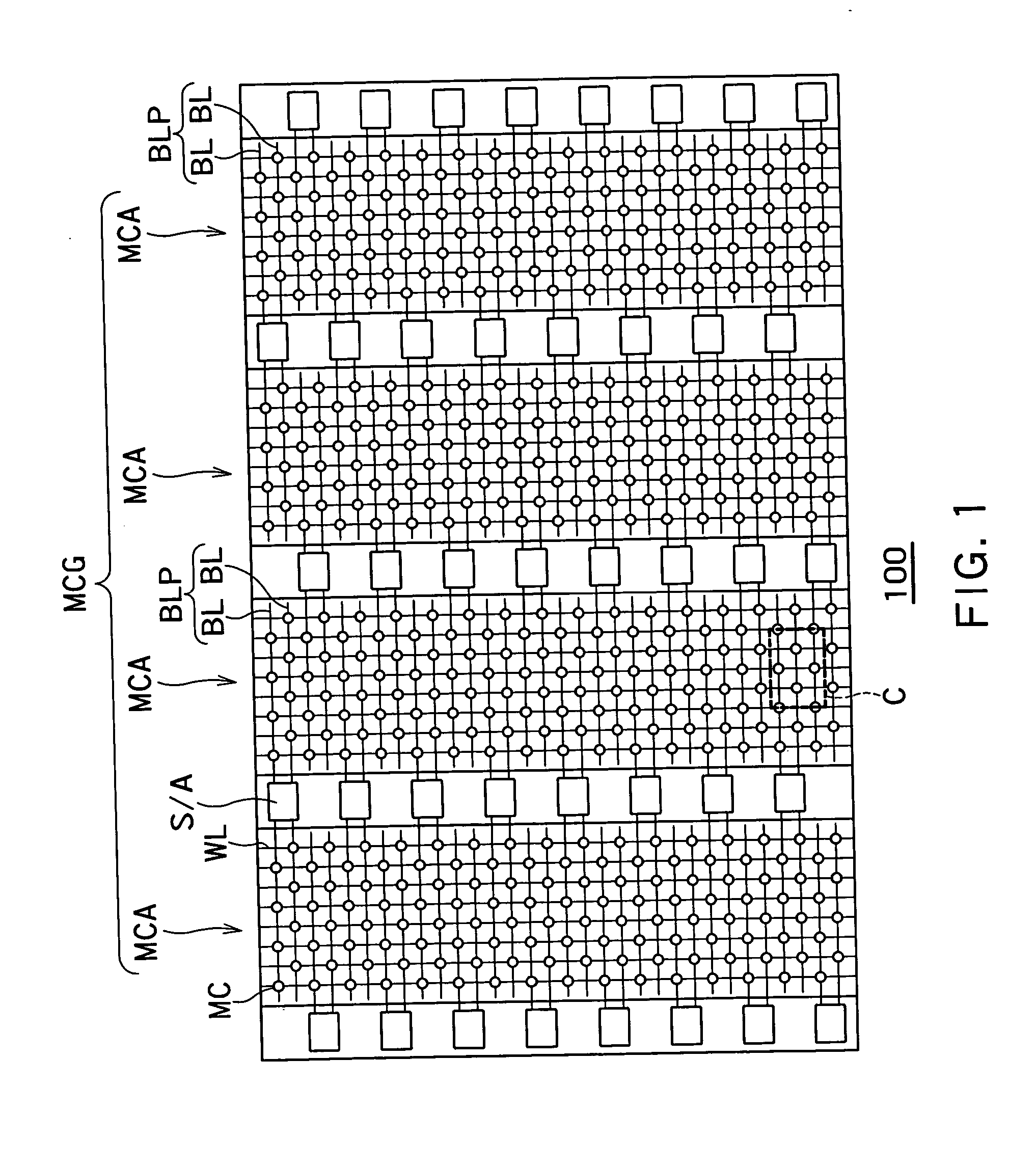
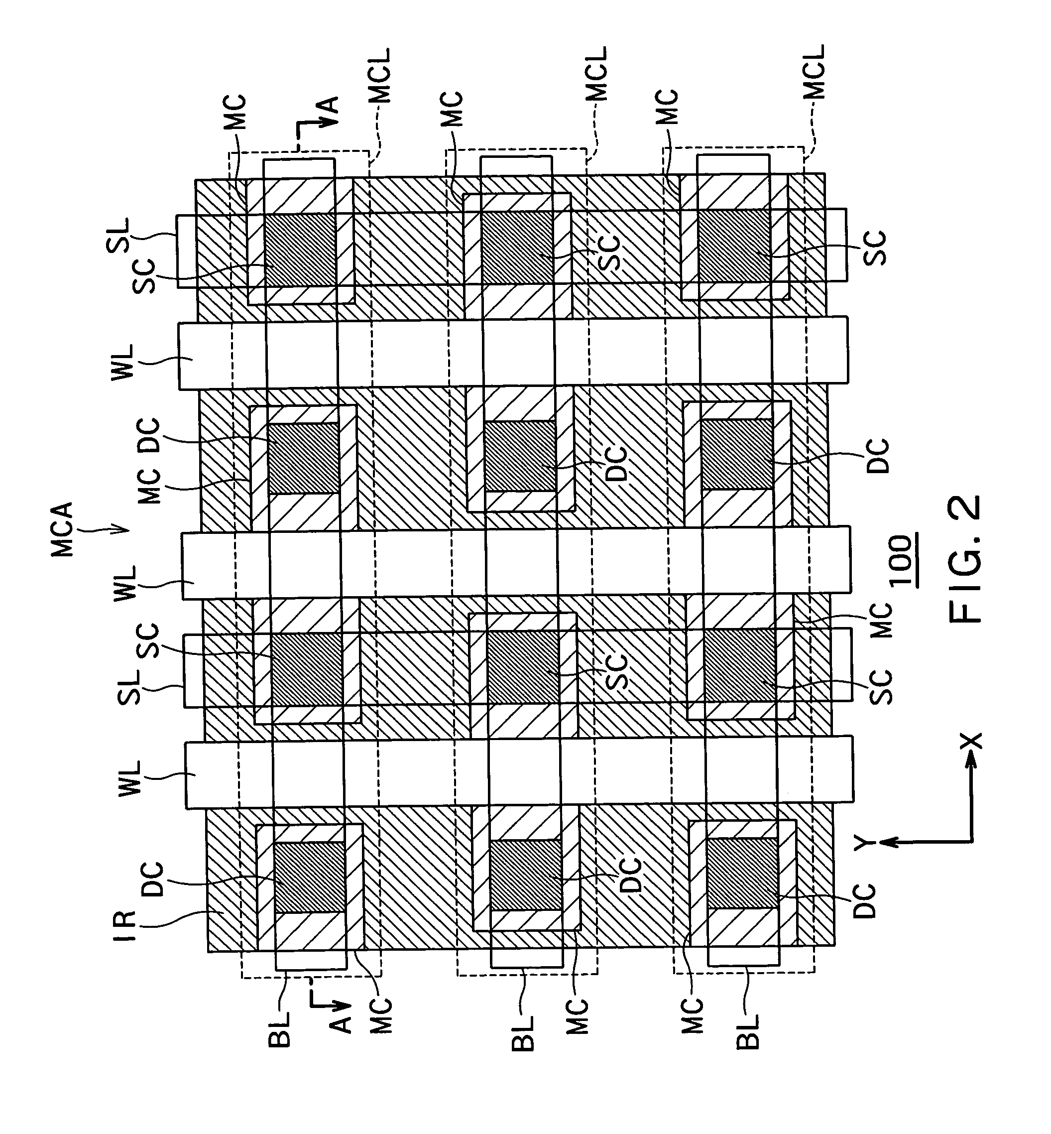
[0021]FIG. 1 is a plan view of an FBC memory device 100 according to the first embodiment of the invention. FIG. 1 illustrates one memory array group MCG including four FBC memory cell arrays MCA. Each memory cell array MCA includes a plurality of memory cells MC. Between every adjacent memory cell arrays MCA and at opposite ends of the memory array group MCG, sense amplifiers S / A are located. The sense amplifiers S / A are connected individually to bit line pairs BLP each having two adjacent bit lines BL in a common memory cell array. Sense amplifiers S / A located between adjacent memory cell arrays MCA are connected to such bit line pairs of the memory cell arrays at opposite sides thereof. That is, four bit lines BL (two bit line pairs BLP) are connected to each sense amplifier S / A. The sense amplifiers S / A have transfer gates each capable of connecting the sense amplifier S / A to one of two bit line pairs BLP at different timings.

[0022] In the first embodiment, one word line WL dri...

second embodiment

[0044]FIG. 4 is a cross-sectional view of an FBC memory device 200 according to the second embodiment of the invention. The FBC memory device 200, in its plan view, appears equally to FIG. 2. The second embodiment is different from the first embodiment in the double-layered structure of the word lines. The FBC memory device 200 includes word lines WL1 in the first layer and word lines WL2 in the second layer. The word lines WL1 lie on the body regions 35 whereas the word lines WL2 lie on bit lines BL in parallel with the word lines WL1. The word lines WL2 are electrically connected to the word lines WL1 at positions in predetermined intervals.

[0045] To reduce the difference in work function between the word lines WL1 and the SOI layer 30, the word lines WL1 are preferably made of a material of the same quality as that of the SOI layer 30. If the SOI layer 30 is made of silicon single crystal, then the word lines WL1 are preferably made of doped polysilicon.

[0046] In this case, how...

third embodiment

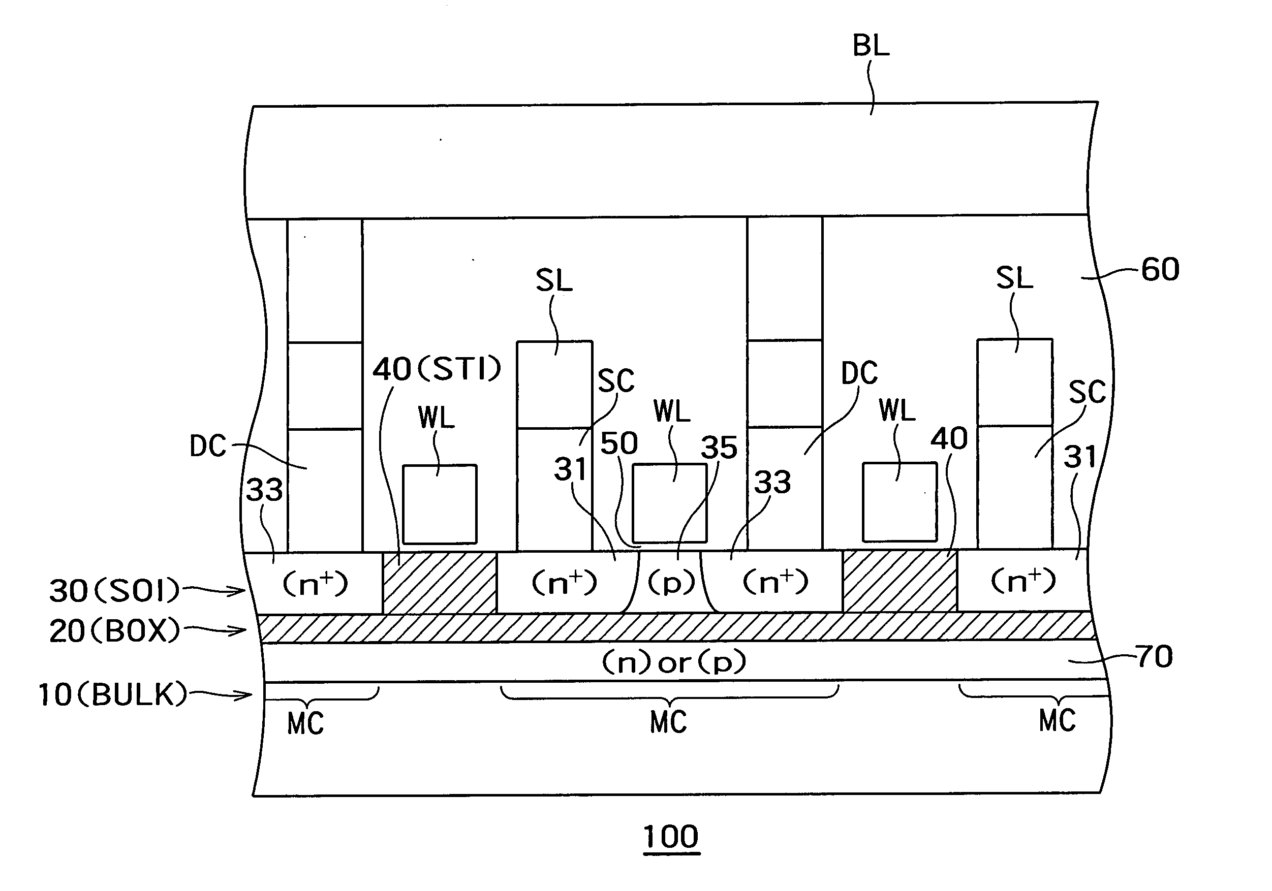
[0048]FIG. 5 is a cross-sectional view of an FBC memory device 300 according to the third embodiment of the invention. In this embodiment, the FBC memory cell portion is formed in SOI, and the peripheral circuit or logic circuit is formed in the bulk. In the third embodiment, the FBC memory cell portion may be configured according to the first or the second embodiment.

[0049] In the FBC memory cell portion, a BOX layer 20 is formed on a bulk 10, and a SOI layer 30 is formed on the BOX layer 20. Since memory cells MC are formed in the SOI layer 30, they are electrically insulated from the bulk 10. Thus, the body regions 35 can float electrically.

[0050] The BOX layer 20 is not formed in the peripheral circuit or logic circuit, and p-type FETs and n-type FETs are formed in a well diffusion layer formed in the bulk 10. Although FIG. 5 shows only one p-type FET and only one n-type FET, a number of these FETs can be combined to make a logic circuit necessary for the peripheral circuit or...


PUM


Abstract

A semiconductor storage device comprises a semiconductor substrate; an insulating layer formed on the semiconductor substrate; a first semiconductor layer formed on the insulating layer and insulated from the semiconductor substrate; memory cells each having a source region of a first conduction type and a drain region of the first conduction type both formed in the first semiconductor layer, and having a body of a second conduction type formed in the first semiconductor layer between the source region and the drain region, said memory cells being capable of storing data by accumulating or releasing electric charge in or from their respective body regions; memory cell lines each including a plurality of said memory cells aligned in the channel lengthwise direction; and a memory cell array including a plurality of said memory cell lines aligned in a channel widthwise direction of the memory cells, wherein said memory cells on a common memory cell line are aligned to uniformly orient the directions from their source regions to the drain regions whereas directions of said memory cells from their source regions to the drain regions on said memory cell line are opposite from those of memory cells on neighboring said memory cell lines.

Description

CROSS-REFERENCE TO RELATED APPLICATIONS [0001] This application is based upon and claims the benefit of priority from the prior Japanese Patent Application No. 2004-56298, filed on Mar. 1, 2004, the entire contents of which are incorporated herein by reference. BACKGROUND OF THE INVENTION [0002] 1. Field of the Invention [0003] This invention relates to a semiconductor storage device. [0004] 2. Related Background Art [0005] Conventional 1T-1C (one transistor-one capacitor) type DRAM cells are getting more and more difficult to fabricate along with their progressive microminiaturization. As their substitutes, FBC memory cells have been proposed. In FBC memory cells, since a single MIS (Metal Insulator Semiconductor) FET constitutes each unit element for storing one-bit information, the area one cell occupies is small. Therefore, FBC memory cells make it possible to form a larger-capacity storage element in a unit area (see Japanese Patent Laid-open Publications JP-2003-68877, JP-2002...

Claims


Application Information

Patent Timeline
Patent Type & Authority Applications(United States)
IPC IPC(8): G11C11/401H01L21/762H01L21/76H01L21/8242H01L27/10H01L27/108H01L27/12H01L31/119
CPCH01L27/108H01L29/7841H01L27/10894H10B12/00H10B12/09
Inventor OHSAWA, TAKASHI
Owner KK TOSHIBA
Why Eureka
Try Eureka