
Optical element, spectroscope and condenser

Active Publication Date: 2005-09-01
NIKON CORP
View PDF4 Cites 2 Cited by
  • Summary
  • Abstract
  • Description
  • Claims
  • Application Information

AI Technical Summary

Benefits of technology

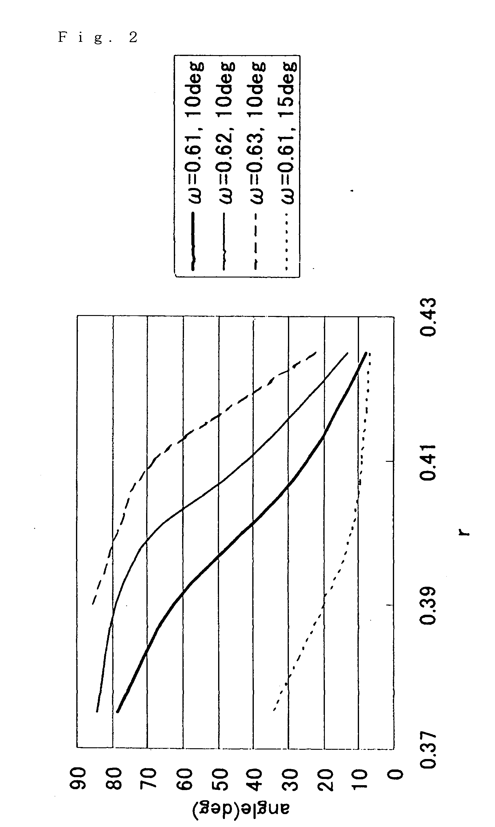
[0011] In a photonic crystal, in cases where a modulation is added to the periodic structure, the band structure is generally no longer formed. However, in cases where the modulation is extremely small, a state is produced in which the basic band structure itself is preserved, and an extremely small perturbation is added to this. Under such conditions, the variation in the band itself is also extremely small; accordingly, the velocity and direction of advance of the light are gradually varied inside the crystal. Furthermore, as in cases where the refractive index continuously varies inside an ordinary medium, there is basically no loss due to reflection or the like.
[0030] If the angle formed by the direction of incidence of the light that is the object of light gathering on the photonic crystal and the first axis is set at 45° or greater, the degree of dispersion of the incident light with respect to first axis increases. Accordingly, the degree of variation in the photonic crystal in the position of incidence of the light can be increased, so that light can be efficiently gathered.

Problems solved by technology

Accordingly, photonic crystals are not always suitable for the precise control of light.
Accordingly, in ordinary photonic crystals, the possibility of splitting light is limited to the splitting of light in an extremely narrow band.
Furthermore, photonic crystals tend to show a loss caused by reflection, scattering, and the like at the boundaries with ordinary substances and other photonic crystals.
This loss tends to be especially large in cases where abnormal dispersion is generated, and it is difficult to avoid such problems.

Method used


Image

  • Optical element, spectroscope and condenser
  • Optical element, spectroscope and condenser
  • Optical element, spectroscope and condenser

Examples


Embodiment Construction

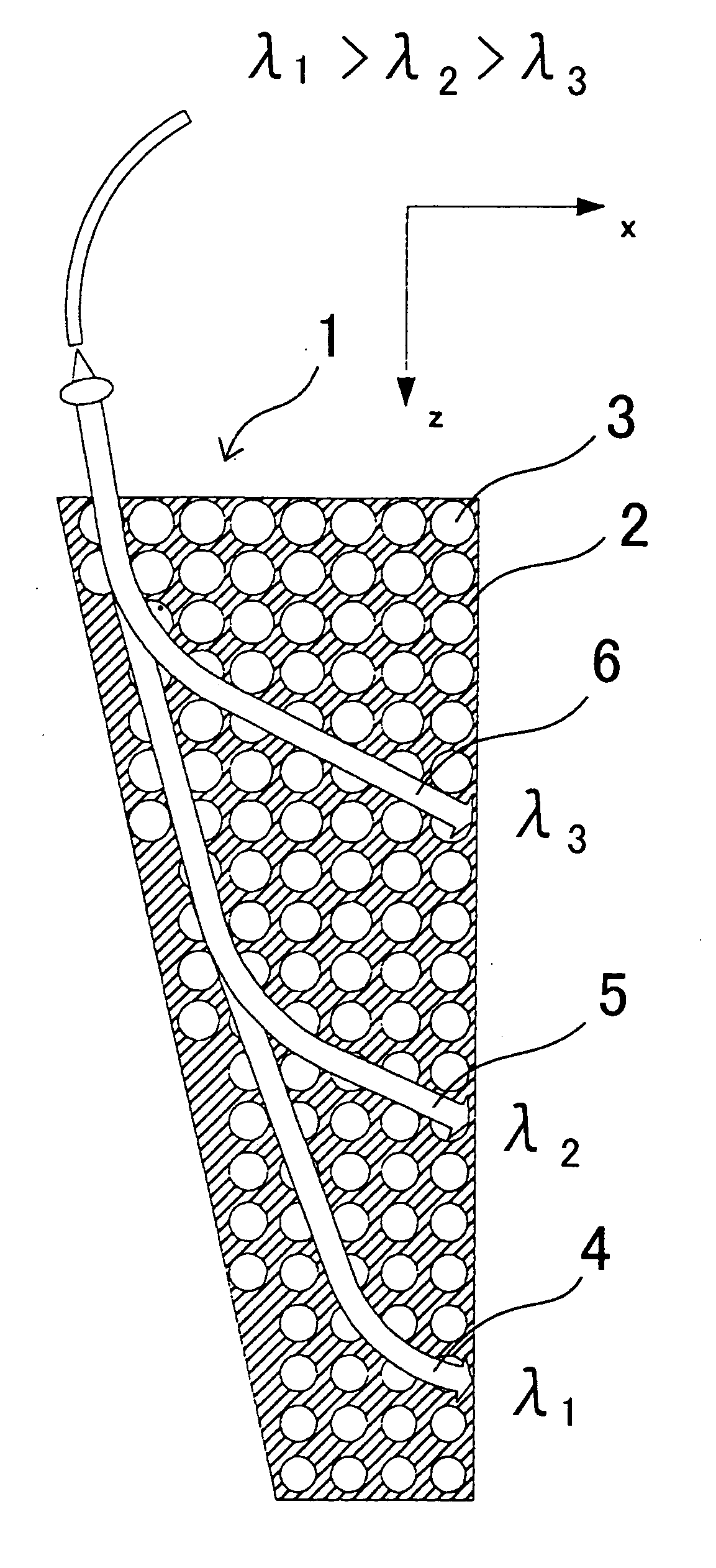
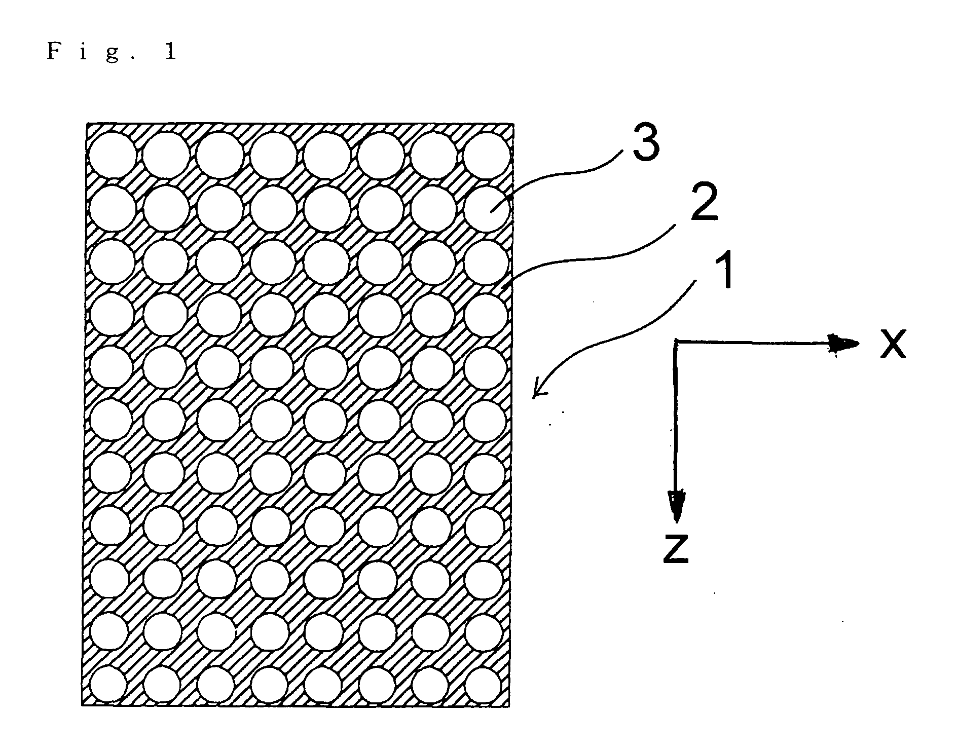
[0036] Working configurations of the present invention will be described below with reference to the figures. FIG. 1 is a diagram showing an outline of the structure of a photonic crystal which forms an optical element constituting one example of a working configuration of the present invention. This photonic crystal 1 has a two-dimensional structure, and has a shape in which round air holes 3 are arranged in the configuration of a square lattice in a medium 2 consisting of BN (boron nitride). If the left-right direction in the plane of the page is taken as the x axis, the vertical direction in the plane of the page is taken as the z axis, and the direction perpendicular to the plane of the page is taken as the y axis, then the air holes 3 are formed in the direction of the y axis inside the photonic crystal 1.

[0037] The refractive index, lattice period, and the like of the medium 2 are constant; however, the size of the air holes 3 gradually varies in the direction of the z axis. ...


PUM


Abstract

In a photonic crystal 1, the refractive index of the medium 2, the period of the lattice, and the like are fixed; however, the size of the air holes 3 gradually varies in the direction of the z axis. Almost all of the light 4 with a vibration number in the vicinity of 0.61 advances directly at the time of incidence on the crystal; however, the direction of advance varies as the size of the holes decreases. On the other hand, as the vibration number increases, the optical path of the light is greatly bent as shown in 5 and 6. Accordingly, a large variation in the angle of refraction can be caused to occur in light with an extremely small wavelength range, so that light splitting with a good resolution can be accomplished.

Description

[0001] This is a continuation from PCT International Application No. PCT / JP2003 / 012480 filed on Sep. 30, 2003, which is hereby incorporated by referenceTECHNICAL FIELD [0002] The present invention relates to an optical element based on a photonic crystal, and a spectroscopic device and a light gathering device using this optical element. BACKGROUND ART [0003] In most cases, high-performance optical elements which are extremely small are required in optical circuits and the like. In recent years, techniques in which photonic crystals are used in such microscopic optical elements have been widely researched. It is known that photonic crystals have extreme properties such as the complete reflection of light regardless of the direction of incidence due to a photonic band gap, variation in the velocity and direction of light due to abnormal dispersion, and that such crystals have numerous properties that are convenient for controlling light. Such photonic crystals and applications of pho...

Claims


Application Information

Patent Timeline
IPC IPC(8): G01J3/14G02B1/02G02B5/04G02B5/18G02B5/28G02B6/12G02B6/122
CPCG02B6/1225B82Y20/00
Inventor TSUKAMOTO, HIROYUKI
Owner NIKON CORP
Learn More