Optical transceiver module

a technology of optical transceiver and module, which is applied in the direction of coupling device connection, semiconductor/solid-state device details, instruments, etc., can solve the problems of no decisive measures taken in connection with optical transceiver modules, gnd potential becomes unstable with an increase in transmission speed, and ld and pd can be stabilized, suppressing electrical crosstalk developing, and enhancing gnd potential.

Inactive Publication Date: 2005-09-01
FUJITSU LTD
View PDF7 Cites 20 Cited by
  • Summary
  • Abstract
  • Description
  • Claims
  • Application Information

AI Technical Summary

Benefits of technology

[0026] According to the present invention, a circuit located between the optical transmission module and the optical receiving module is electrically short-circuited. Accordingly, stability of the GND potential of an optical device, such as an LD and a PD, can be enhanced. The influence of stray capacitance and stray inductance existing in the lead pins, the housings, and the internal components of the optical devices can be suppressed. Consequently, fluctuations in the LD housing (GND) potential, which arise during the high-frequency driving operation, can be suppressed, thereby significantly suppressing the electrical crosstalk developing between the transmission and receiving sections.

Problems solved by technology

However, in a high-frequency range in which the transmission speed exceeds 1.0 Gbps, a GND potential becomes greatly deviated from an ideal potential because of parasitic effects, such as stray capacitance and stray inductance of lead pins, housings, and internal components of optical devices, such as a laser diode (LD) and a photodiode (PD).
However, no decisive measures have been taken in connection with an optical transceiver module which is chiefly typified by a CAN-type optical transceiver module and in which an LD module and a PD module are formed integrally.
Therefore, it is understood that the GND potential becomes unstable with an increase in transmission speed and that the fluctuations in the GND potential and the crosstalk become greater.
The transmission and receiving sections are susceptible to the influence of noise.
For these reasons, electrical crosstalk developing between the transmission and receiving sections is great, which is responsible for deterioration of receiving sensitivity.
However, a distance of about 1 cm is required at 2.4 Gbps, and hence it is considered that this optical transceiver module cannot be implemented through use of a current compact optical transceiver module.
During high-frequency driving operation, high-frequency noise deriving from the high-frequency driving operation also induces deterioration of the waveform of the light output from the transmission section.
However, the technique fails to suppress the electrical crosstalk developing between the transmission and receiving sections of the optical transceiver module in which the LD module 100, the PD module 200, and the circuit board 300 are formed integrally.

Method used


Image

  • Optical transceiver module
  • Optical transceiver module
  • Optical transceiver module

Examples


first embodiment

[A] Descriptions of a First Embodiment

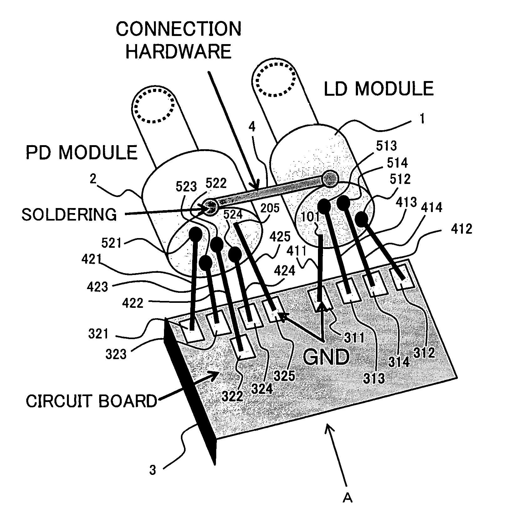
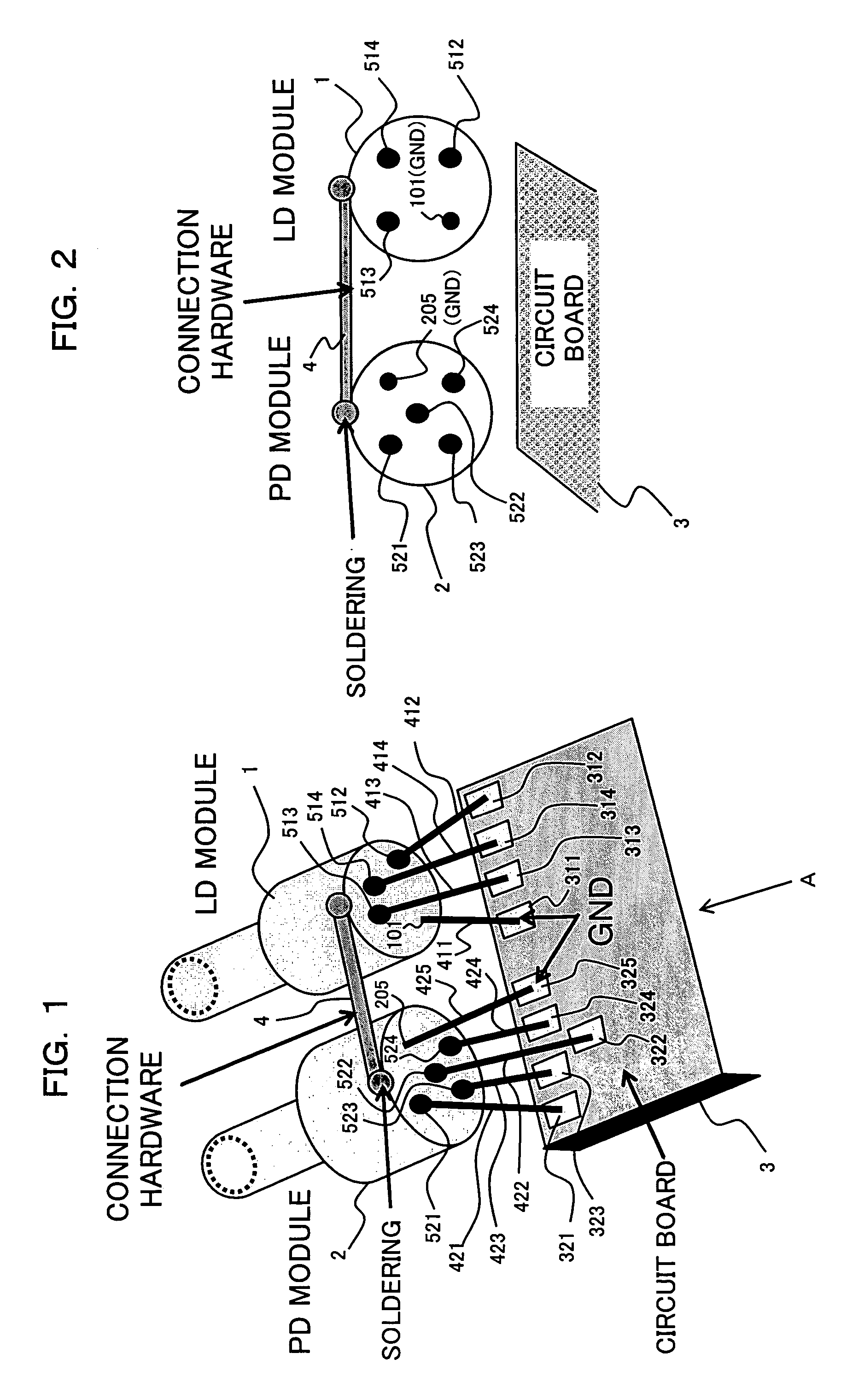
[0041]FIG. 1 is a diagrammatic perspective view showing the configuration of an optical transceiver module serving as a first embodiment of the present invention. FIG. 2 is a diagrammatic front view of the optical transceiver module when viewed in a direction of arrow A shown in FIG. 1. As shown in FIGS. 1 and 2, the optical transceiver module of the present invention comprises a CAN-type LD module 1 which has an LD (a light-emitting element) provided in a cylindrical metal housing and acts as an optical transmission module; a CAN-type PD module 2 which has a PD (a light-receiving element) provided in a cylindrical metal housing and acts as an optical receiving module; and a circuit board (a drive circuit board) 3 for driving the LD module 1 and the PD module 2. In the same manner as in the case of the optical transceiver module described by reference to FIGS. 10 and 11, the LD module 1 is connected to the circuit board 3 (LD connection terminal...

second embodiment

[B] Descriptions of a Second Embodiment

[0051]FIG. 4 is a diagrammatic perspective view showing the configuration of an optical transceiver module serving as a second embodiment of the present invention, and FIG. 5 is a diagrammatic front view of the optical transceiver module when viewed in a direction of arrow A shown in FIG. 4. As shown in FIGS. 4 and 5, the optical transceiver module of the present invention comprises the CAN-type LD module 1; the CAN-type PD module 2; the circuit board (drive circuit board) 3; and another circuit board (sub-circuit board) 5.

[0052] The modules 1, 2 are mounted on one surface of the sub-board (module mount board) 5. Formed in the other surface of the sub-board are hole sections (through holes) 51 to 54 and 61 to 65 for use with (and which are aligned with) the lead pins 411 to 414 and 421 to 425 of the respective modules 1, 2. A GND pattern 50 having a wide area is formed over the entirety or substantially the entirety of other surface of the sub...

second modification

(B2) Descriptions of a Second Modification

[0062]FIG. 7 is a diagrammatic front view showing the configuration of a second modification of the optical transceiver module described by reference to FIGS. 4 and 5. In the optical transceiver module shown in FIG. 7, provided on the sub-board 5 are the LD anode electrode pattern 55; an electrode section 56 (LD cathode electrode pattern) to which the LD cathode lead pin 513 (LD cathode terminal 103) is to be connected by means of soldering or the like; an electrode pattern 57 to be used for connecting the LD anode electrode pattern 55 to the LD cathode electrode pattern 56; a capacitor 7 interposed between the LD anode electrode pattern 55 and the electrode pattern 57 by means of soldering or the like; a resistor 8 interposed between the LD cathode electrode 56 and the electrode pattern 57 by means of soldering or the like; and the GND pattern 50 formed so as to avoid the electrode patterns 55, 56, 57, the capacitor 7, and the resistor 8.

[...


PUM


Abstract

An optical transceiver module is constituted so as to have an optical transmission module, an optical receiving module, a drive circuit board for driving the optical transmission module and the optical receiving module, and short-circuit means which induces an electrical short circuit between housings of the respective modules or induces an electrical short circuit between ground (GND) terminals of the respective modules on the module sides with respect to the drive circuit board. As a result, in the optical transceiver module, stray capacitance and stray inductance in lead pins, housings, and internal components of optical devices, such as an LD and a PD, are removed, thereby suppressing fluctuations in the potential (GND) of an LD housing which arise during high-frequency driving operation, as well as considerably suppressing electrical crosstalk between the transmission and receiving modules.

Description

BACKGROUND OF THE INVENTION [0001] (1) Field of the Invention [0002] The present invention relates to an optical transceiver module, and more particularly, to a technique suitable for use in a compact optical transceiver module in which components (e.g., an LD, a PD, and a circuit board) to be used for optical fiber communication are integrally constituted and which is subjected to high-frequency driving. [0003] (2) Description of the Related Art [0004] In a conventional optical transceiver module whose transmission speed is low [1.0 Gbps (gigabits / second) or less], electrical crosstalk arising between a transmission section and a receiving section can be lessened by means of upgrading a GND (ground) on a drive circuit board. However, in a high-frequency range in which the transmission speed exceeds 1.0 Gbps, a GND potential becomes greatly deviated from an ideal potential because of parasitic effects, such as stray capacitance and stray inductance of lead pins, housings, and intern...

Claims


Application Information

Patent Timeline
Patent Type & Authority Applications(United States)
IPC IPC(8): G02B6/42H01L23/04H01L27/14H01L27/15H01L31/02H01L31/0232H01R4/02H01S5/022H01S5/026
CPCG02B6/4201G02B6/4246H01R13/6461H01R4/021G02B6/4277H01L2924/19107
Inventor NAKAMOTO, KEN-ICHIAKASHI, TAMOTSUMORI, KAZUYUKISAKURAMOTO, SHIN-ICHI
Owner FUJITSU LTD
Why Eureka
Try Eureka