High voltage device embedded non-volatile memory cell and fabrication method

a high-voltage device and memory cell technology, applied in the direction of semiconductor/solid-state device manufacturing, semiconductor devices, electrical equipment, etc., can solve the problem of insufficient process window

Inactive Publication Date: 2005-09-08
TAIWAN SEMICON MFG CO LTD
View PDF15 Cites 16 Cited by
  • Summary
  • Abstract
  • Description
  • Claims
  • Application Information

AI Technical Summary

Benefits of technology

[0013] Also in accordance with the objects of the invention, a method for fabricating a symmetrical high voltage integrated circuit structure is achieved. An n-well is formed within a substrate in a channel area. A high voltage p-well is formed within the substrate in a drain area wherein the drain area is located on one side of the channel region. A high voltage p-well is formed within the substrate in a source area wherein the source area is located on the other side of the channe...

Problems solved by technology

There are two major challenges with HVPMOS devices.
One is that the process window is not large enough.
Another ...

Method used


Image

  • High voltage device embedded non-volatile memory cell and fabrication method
  • High voltage device embedded non-volatile memory cell and fabrication method

Examples


Embodiment Construction

of THE PREFERRED EMBODIMENTS

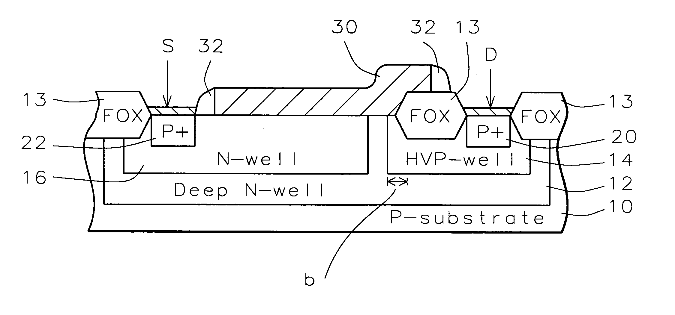
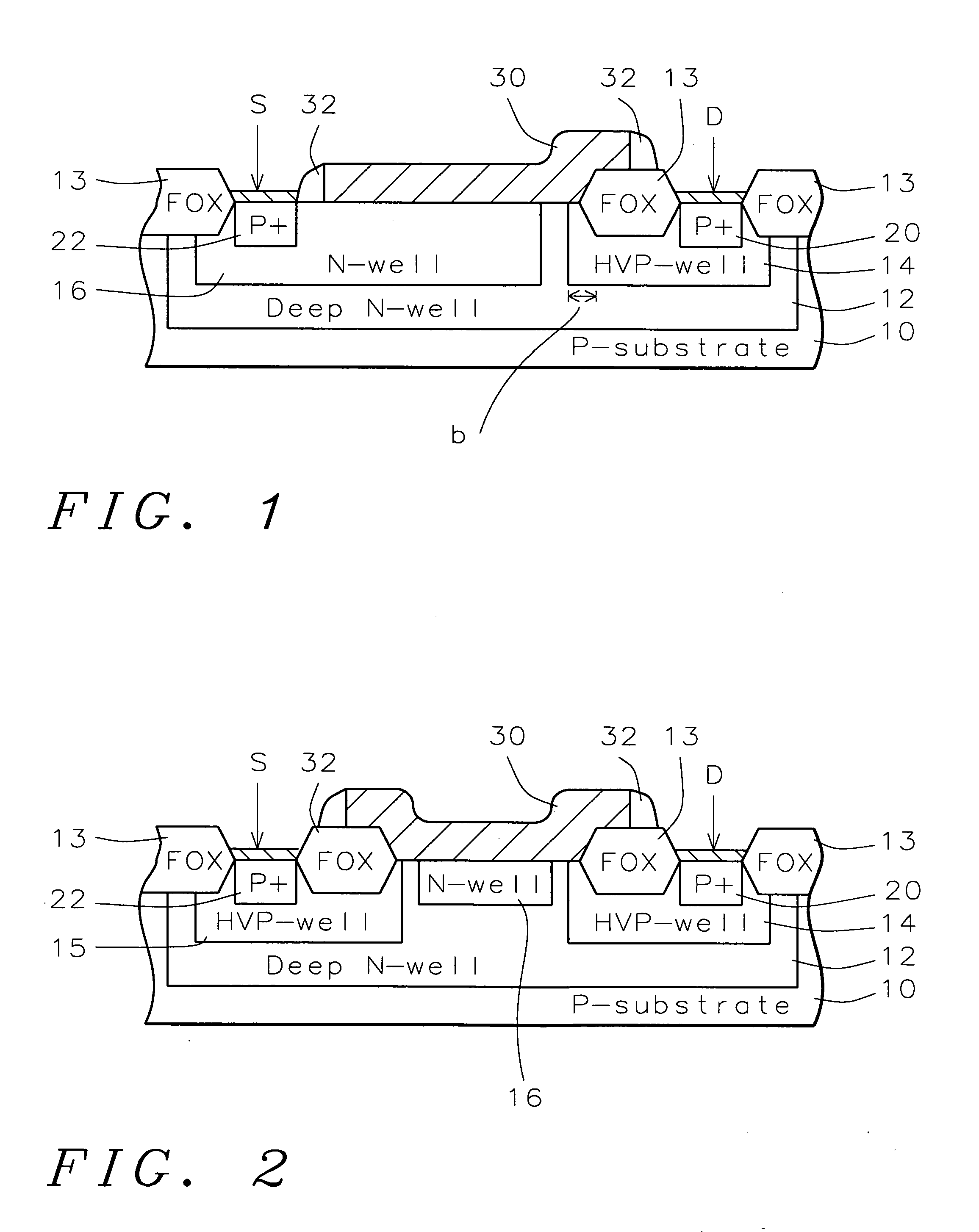
[0017] The present invention provides a device and fabrication method for an improved high voltage PMOS device, providing an enlarged process window and an increased device breakdown voltage. This is achieved by inserting an extra n-well in the source side and the substrate underlying the gate electrode of the high voltage PMOS device to improve HV device breakdown. The process of the present invention is fully compatible with the conventional process without increased process cost. Two preferred embodiments of the present invention will be described. FIG. 1 shows an asymmetrical high voltage device while FIG. 2 shows a symmetrical device.

[0018]FIG. 1 is an illustration of an asymmetrical PMOS structure. P-substrate 10 is shown. Deep n-well 12 has been formed within the substrate. Isolation regions such as field oxide (FOX) regions 13 are formed in and on the substrate to separate active areas. A high voltage P-well 14 is typically formed in the drain si...


PUM


Abstract

A high voltage PMOS device having an improved breakdown voltage is achieved. An asymmetrical high voltage integrated circuit structure comprises a gate electrode on a substrate and source and drain regions within the substrate on either side and adjacent to the gate electrode wherein the source region is encompassed by an n-well. A symmetrical high voltage integrated circuit structure comprises a gate electrode on a substrate, source and drain regions within the substrate on either side and adjacent to the gate electrode, and an n-well in the substrate underlying the gate electrode. The n-well in both structures shifts the breakdown point from the silicon surface to the bottom of the source or drain regions.

Description

BACKGROUND of the INVENTION [0001] 1. Field of Invention [0002] This invention is directed to a method of fabricating a high voltage PMOS device and more particularly to a method of fabricating a high voltage PMOS device having n-type source side doping in the manufacture of integrated circuits. [0003] 2. Description of Related Art [0004] High voltage PMOS (HVPMOS) devices have a high breakdown voltage. There are two major challenges with HVPMOS devices. One is that the process window is not large enough. The overlay between the P-well and the active area must be at least 0.6 μm. Another challenge is in achieving a high enough breakdown voltage, for example, as much as 40 volts for a p-substrate wafer. [0005] U.S. Pat. No. 5,578,855 to Gauffer et al describes a high voltage device having source and drain within an n-well and a p-field extension below the drain. U.S. Pat. No. 4,442,591 to Haken shows a high voltage device having both a source and a drain within a p-well and within an...

Claims


Application Information

Patent Timeline
IPC IPC(8): H01L31/113
CPCH01L29/1045H01L29/7835H01L29/456H01L29/42368
Inventor TSAI, HUNG-CHIHCHOU, CHIEN-CHIHCHANG, YING-TINGCHU, CHE-JUNGLIU, KUO-CHIO
Owner TAIWAN SEMICON MFG CO LTD
Why Eureka
Try Eureka