Devices with adjustable dual-polarity trigger- and holding-voltage/current for high level of electrostatic discharge protection in sub-micron mixed signal CMOS/BiCMOS integrated circuits

a technology of cmos/bicmos and integrated circuits, which is applied in the direction of semiconductor devices, diodes, transistors, etc., can solve the problems of low level of protection, affecting the reliability and functionality of semiconductor integrated circuits, and the current devices of advanced silicided cmos/bicmos technologies for high level of esd protection are unavailable, so as to achieve high protection

Inactive Publication Date: 2009-07-28
INTERSIL INC +1
View PDF28 Cites 79 Cited by
  • Summary
  • Abstract
  • Description
  • Claims
  • Application Information

AI Technical Summary

Benefits of technology

[0017]In accordance with various embodiments of the invention, there is a method and a device comprising a multifinger device structure with interleaved ballast resistance and interdigited metal, optimized for high current distribution, low risk of filamentation that is versatile to adapt to demanding layout rules, and packaging constraints of high density integrated circuits.
[0021]In accordance with various embodiments of the invention, there is a method and a device that can afford the migration of existing products to advanced CMOS / BiCMOS technologies to take further advantage of the technology downscaling tendency, while providing the required level of ESD-induced damage immunity.
[0022]In accordance with various embodiments of the invention, there is a method and a device for multi-transmitters / multi-receivers and multi-protocols data communication chips in general, that provide high levels of protection from damage causes by very high levels of positive and negative ESD pulses. According to the invention, this can be achieved by providing dual-polarity ground-referenced ESD protection circuits at the communication pads, protection at the low voltage-low ESD digital pads, and asymmetric dual-polarity protection at every power supply rail on a chip.

Problems solved by technology

The occurrence of high voltage spikes, namely electrostatic discharge (ESD), induced by uncontrollable charge imbalance between a chip's input or output pads and externally grounded or pre-charged objects, affects the reliability and functionality of semiconductor integrated circuits (ICs), commonly resulting in hard-failure for advanced technologies.
A major problem, however, is that current devices for advanced silicided CMOS / BiCMOS technologies for high level of ESD protection purpose are unavailable.
Further, standard devices, optimized for performance not for power, are ineffective in handling the high power obtained during an ESD event.
The shrinking of device dimensions in advanced technologies, aimed at both high performance and high density circuits, often results in ICs that are more sensitive to ESD events.
This consequence of the driving technology downscaling is mainly associated with different tradeoffs that improve performance by decreasing the power handling capability.
Moreover, increasing the size of the traditional protection structures to levels comparable with the core circuit dimensions does not guarantee that the ESD protection requirements are reached.
This condition can degrade the ESD performance in sub-micron mixed-signal ICs and diminish the potential advantages of the technology downscaling.
This ability is commonly called “5 volt friendly.” This alternative ESD solution is directed to a very close interface voltage and does not provide a solution for a circuit that should operate at voltage range exceeding three or more times the power supply.
Moreover, they can be very sensitive to the technology design rules.
There are several known disadvantages of this system, however.
For example, parallel / series clamping diodes require a large area, are slow-response, exhibit undesirable parasitic capacitance and leakage current, and have undesirably high “on” resistance.
Also, such large diode clamps require a low impedance return path.
Additionally, large clamping devices are not standard devices and are not practiced in advanced high density integrated circuits.
As such, it is limited to only a few processes that provide this flexibility.
This increases the risk of hot spot generation and non-uniform current distribution when dimensions in the device are increased for higher levels of ESD protection which poses scaling problems.
A further limitation of the device is its inability to provide asymmetric dual polarity characteristics and non-uniform operating condition in a parallel device array.

Method used


Image

  • Devices with adjustable dual-polarity trigger- and holding-voltage/current for high level of electrostatic discharge protection in sub-micron mixed signal CMOS/BiCMOS integrated circuits
  • Devices with adjustable dual-polarity trigger- and holding-voltage/current for high level of electrostatic discharge protection in sub-micron mixed signal CMOS/BiCMOS integrated circuits
  • Devices with adjustable dual-polarity trigger- and holding-voltage/current for high level of electrostatic discharge protection in sub-micron mixed signal CMOS/BiCMOS integrated circuits

Examples


second embodiment

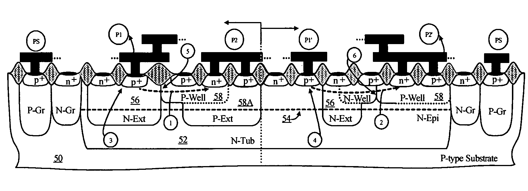
[0100]FIG. 17 shows a second embodiment for a symmetric DP-STT ESD protection device for a circuit operating at a bipolar I / O voltage range of about to ±25 V. Similar to the description provided for FIG. 14, there are symmetric sub-sections (160 and 162), in this case p-type MDSTT-1 (Table 3B), each of them providing ESD protection for current flowing in the opposite directions. The P1 / N2 / P2 / N1 structure defined for each subsection present a combination of forward and reverse blocking junctions, 166 and 164, that give rise to the I-V characteristics shown in FIG. 18. The forward and reverse I-V characteristics 456 and 452, respectively, are obtained for a two-section one-finger 200 μm width device. The symmetric trigger voltage, 454 and 450 in FIG. 18, are measured very close to the established ±25 V, while the device conductivity modulation is ideal for ESD protection without latchup problems.

third embodiment

[0101]FIG. 19 shows a third embodiment for still higher trigger voltages. This cross-sectional view depicts a single finger DP-STT for symmetric trigger voltage over ±30 V. This embodiment maintains the general scheme of the two previous embodiments, but the sub-section blocking junctions are defined differently, see sub-sections 170 and 172, corresponding to an embodiment of the p-type MDSTT (P-MDSTT-2 in Table 3B). The forward blocking junction 176 is graded by the low doping concentration of the N−Epi 54. The reverse blocking junction 174 allows for conduction of the device without interaction between the parasitics formed with the p-side of the guard ring 168 and the device's electrodes, 180 and 182. FIG. 20 shows the resulting symmetric TLP I-V characteristics, 462 and 468, for a five finger device using the inter-finger guard ring isolation. The forward and reverse trigger voltages, 464 and 458, are close to ±36 V and the currents at the holding voltages, 460 and 466, are over...


PUM


Abstract

Symmetrical / asymmetrical bidirectional S-shaped I-V characteristics with trigger voltages ranging from 10 V to over 40 V and relatively high holding current are obtained for advanced sub-micron silicided CMOS (Complementary Metal Oxide Semiconductor) / BiCMOS (Bipolar CMOS) technologies by custom implementation of P1-N2-P2-N1 / / N1-P3-N3-P1 lateral structures with embedded ballast resistance 58, 58A, 56, 56A and periphery guard-ring isolation 88-86. The bidirectional protection devices render a high level of electrostatic discharge (ESD) immunity for advanced CMOS / BiCMOS processes with no latchup problems. Novel design-adapted multifinger 354 / interdigitated 336 layout schemes of the ESD protection cells allow for scaling-up the ESD performance of the protection structure and custom integration, while the I-V characteristics 480 are adjustable to the operating conditions of the integrated circuit (IC). The ESD protection cells are tested using the TLP (Transmission Line Pulse) technique, and ESD standards including HBM (Human Body Model), MM (Machine Model), and IEC (International Electrotechnical Commission) IEC 1000-4-2 standard for ESD immunity. ESD protection performance is demonstrated also at high temperature (140° C.). The unique high ratio of dual-polarity ESD protection level per unit area, allows for integration of fast-response and compact protection cells optimized for the current tendency of the semiconductor industry toward low cost and high density-oriented IC design. Symmetric / asymmetric dual polarity ESD protection performance is demonstrated for over 15 kV HBM, 2 kV MM, and 16.5 kV IEC for sub-micron technology.

Description

CROSS-REFERENCE TO RELATED APPLICATIONS[0001]This application claims priority to U.S. Provisional Patent Application Ser. No. 60 / 696,794 filed on Jul. 7, 2005, the disclosure of which is incorporated by reference in its entirety.FIELD OF THE INVENTION[0002]The subject matter of this application relates to semiconductor integrated circuits. More particularly, the subject matter of this application relates to Electrostatic Discharge (ESD) protection in Complementary Metal Oxide Semiconductor (CMOS) or Bipolar CMOS (BiCMOS) mixed-signal integrated circuits (ICs) operating at Input / Output (I / O) voltages well above / below the native power supply voltage.BACKGROUND OF THE INVENTION[0003]The occurrence of high voltage spikes, namely electrostatic discharge (ESD), induced by uncontrollable charge imbalance between a chip's input or output pads and externally grounded or pre-charged objects, affects the reliability and functionality of semiconductor integrated circuits (ICs), commonly resulti...

Claims


Application Information

Patent Timeline
Patent Type & Authority Patents(United States)
IPC IPC(8): H01L29/74H01L29/76H01L29/94H01L31/062H01L31/111
CPCH01L29/87H01L27/0262
Inventor SALCEDO, JAVIER A.LIOU, JUIN J.BERNIER, JOSEPH C.WHITNEY, DONALD K.
Owner INTERSIL INC
Why Eureka
Try Eureka