
Double-faced field emission display device

a display device and display device technology, applied in the direction of discharge tube luminescnet screens, tubes with electrostatic control, tubes with screens, etc., can solve the problems of inability to control the emission of electrons very accurately, the structure of the field emission display device assembly is complicated, and the cost of the field emission display device assembly is high, etc., to achieve low cost, simple structure, and small bulk

Active Publication Date: 2005-09-08
TSINGHUA UNIV +1
View PDF8 Cites 15 Cited by
  • Summary
  • Abstract
  • Description
  • Claims
  • Application Information

AI Technical Summary

Benefits of technology

[0009] Accordingly, an object of the present invention is to provide a double-faced field emission display device having a simple structure, small bulk, and low cost.
[0012] Compared with a conventional double-faced field emission display device, the double-faced field emission display device of the present invention adopts a pair of fluorescent screens and a single driving system to simultaneously display same images at the two fluorescent screens. Furthermore, a plurality of grid plates are adopted, so that the emitting voltage is low and the emission of the electrons can be controlled accurately. The double-faced field emission display device of the present invention has a simple structure, small bulk and low cost, and can be advantageously applied in traffic signal boards, large-scale display boards, surround cinemas and so on.

Problems solved by technology

Furthermore, a structure of the field emission display device assembly is complicated.
Thus, the field emission display device assembly is bulky and costly.
In addition, the emission of the electrons cannot be controlled very accurately.

Method used


Image

  • Double-faced field emission display device
  • Double-faced field emission display device
  • Double-faced field emission display device

Examples


Embodiment Construction

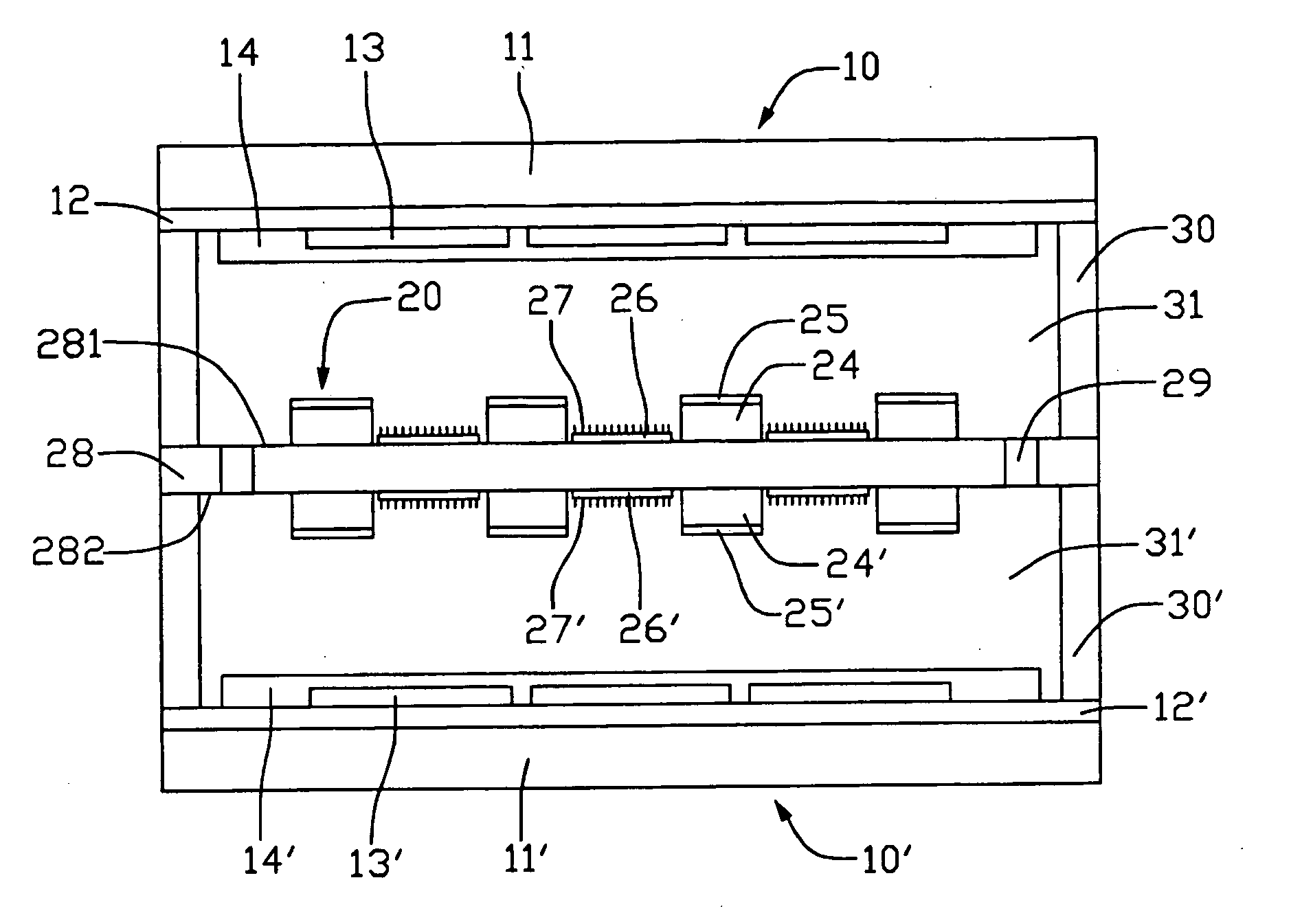
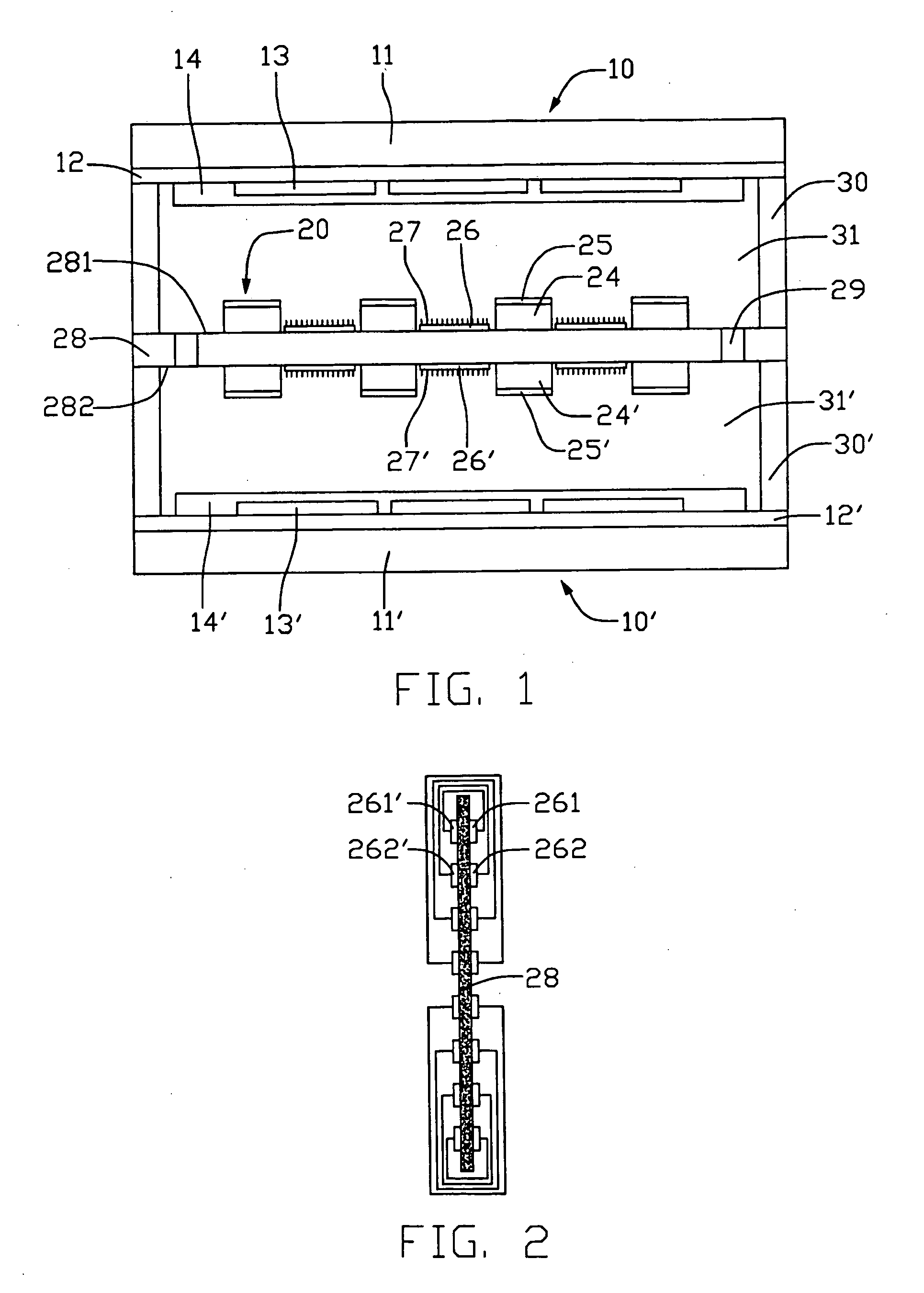
[0018] Referring to FIG. 1, a double-faced field emission display device (not labeled) of the present invention comprises two parallel fluorescent screens 10, 10′, and an electron emission structure 20 located between the fluorescent screens 10, 10′. The fluorescent screen 10 comprises a transparent substrate 11, with an anode plate 12, a plurality of coplanar fluorescent layers 13, and an aluminum film 14 formed at an inner surface (not labeled) of the transparent substrate 10. The anode plate 12 is formed on the inner surface of the transparent substrate 10. The fluorescent layers 13 are coated on the anode plate 12. The aluminum film 14 covers the fluorescent layers 13. The fluorescent layers 13 comprise three primary colors, such as red, green and blue. The fluorescent screen 10′ has substantially the same structure as that of the fluorescent screen 10. The fluorescent screen 10′ comprises a transparent substrate 11′, with an anode plate 12′, a plurality of coplanar fluorescent ...


PUM


Abstract

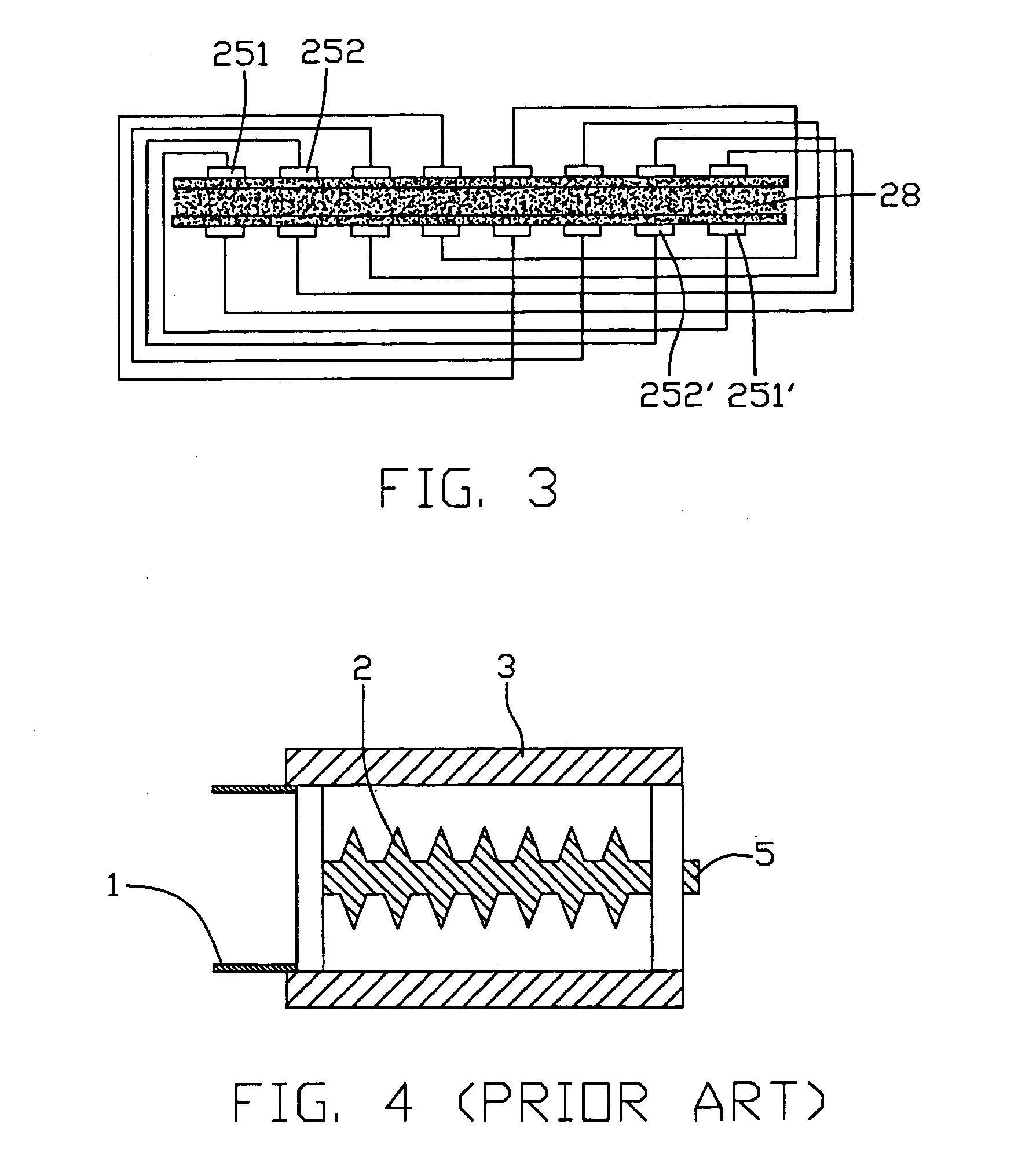
A double-faced field emission display device includes two parallel fluorescent screens (10, 10′) and an electron emission structure (20) located between the fluorescent screens. Each fluorescent screen includes a transparent substrate (21, 21′) with an anode plate (12, 12′) and coplanar fluorescent layers (13, 13′) formed at an inner surface of the transparent substrate. The electron emission structure includes an opaque insulative substrate (28) with cathode plates (26, 26′), electron emitters (27, 27′) and grid plates (25, 25′) formed at each of opposite surfaces (281, 282) thereof. Symmetrically opposite pairs of same electrodes are electrically interconnected so that the fluorescent screens can simultaneous display a same image. Only a single driving system is needed to achieve the simultaneous display.

Description

BACKGROUND OF THE INVENTION [0001] 1. Field of the Invention [0002] The invention relates generally to double-faced display devices, and more particularly to double-faced field emission display devices. [0003] 2. Prior Art [0004] A field emission display device has been widely used in computers, mobile communications and consumer electronics. Conventionally, the field emission display device comprises a fluorescent screen and an electron emission structure. The fluorescent screen comprises an anode plate formed thereat, and the electron emission structure comprises a cathode plate formed thereat. In use, when an emitting voltage is applied between the anode plate and the cathode plate, electrons are emitted from the cathode plate and bombard the fluorescent screen, whereby visible light is produced and an image is displayed on the fluorescent screen. The field emission display device only displays a single image at one surface thereof. [0005] In certain applications, a field emissio...

Claims


Application Information

Patent Timeline
Patent Type & Authority Applications(United States)
IPC IPC(8): H01J1/62H01J31/12
CPCH01J2329/005H01J31/127
Inventor CHEN, PI-JINLIU, PENGQIAN, LIWEI, YANGSHENG, LEI-MEILEI, YOU-HUALIU, LIANGFAN, SHOU-SHAN
Owner TSINGHUA UNIV
Learn More