Metal member and electric contact using same
a metal member and electric contact technology, applied in the field of metal members, can solve the problems of nip alloy plating film low toughness and brittle films, nip alloy plating film may be peeled off, deterioration of corrosion resistance and wear resistance, etc., to achieve excellent wear resistance, increase the life of an electric contact, and reduce the amount of noble metals
- Summary
- Abstract
- Description
- Claims
- Application Information
AI Technical Summary
Benefits of technology
Problems solved by technology
Method used
Image
Examples
example 1
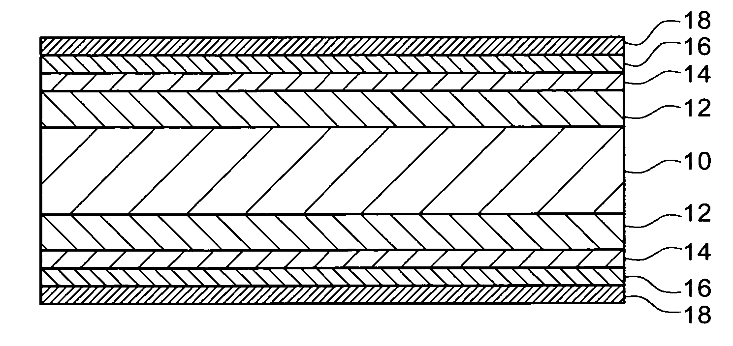
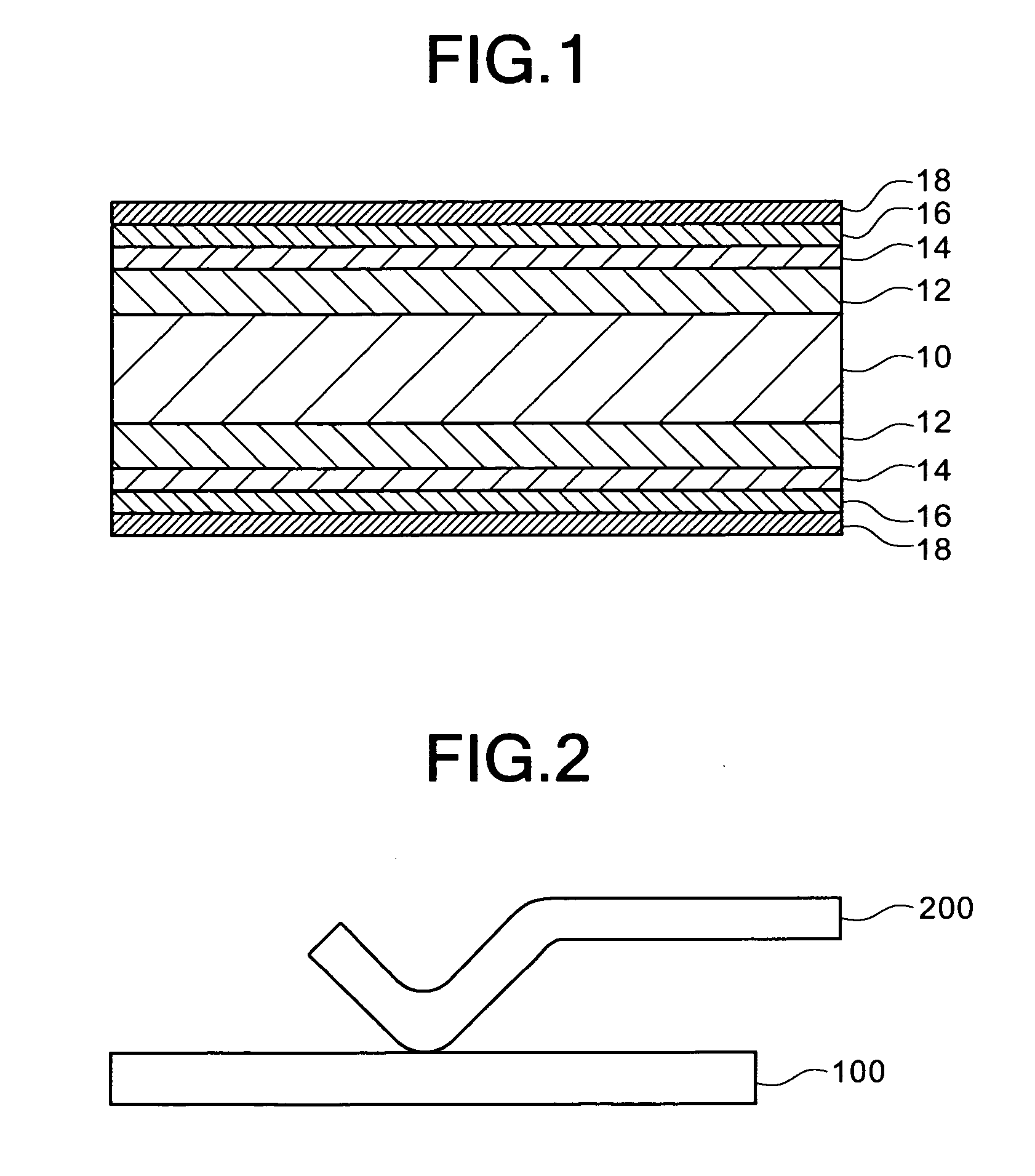
[0053] After a copper plate (C1201P) having a size of 60 mm×60 mm×0.3 mm was prepared as a metal base to pretreated, Ni plating, Cu plating, Ni—P plating and AuCo plating were sequentially carried out, and thereafter, a sealing process was carried out to produce a metal member. These processes will be described below.
Pretreatment
[0054] The above described copper plate was immersed in an alkali degreasing solution, and a voltage of 5 V was applied thereto for two minutes to carry out an electrolytic degreasing process. Thereafter, the copper plate was taken out of the degreasing solution to be washed with pure water. Then, the copper plate was immersed in an aqueous solution containing 5 wt % of sulfuric acid for thirty seconds to carry out an acid cleaning process. Thereafter, the copper plate was taken out of the aqueous sulfuric acid solution to be washed with pure water again.
Ni Plating
[0055] Then, the copper plate thus pretreated and an Ni plate were immersed in a plating ba...
example 2
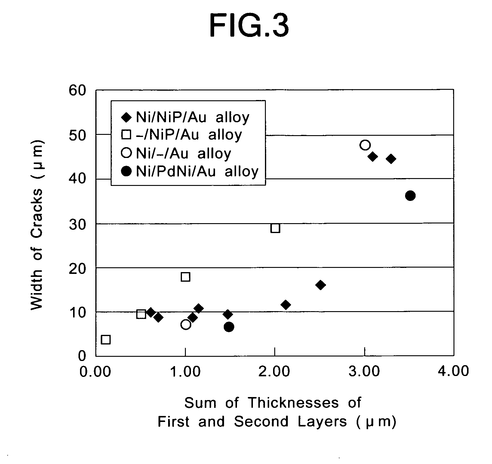
[0063] By the same method as that in Example 1, except that the thickness of the Ni film was 0.5 μm, a metal member was produced, and the wear resistance, bending workability and apparent film hardness thereof were evaluated. As a result, the wear scar width after forty thousand reciprocating motions was 0.10 mm, the mean crack width was 9.8 μm, and the apparent film hardness was 98 Hv.
example 3
[0064] By the same method as that in Example 1, except that the thickness of the Ni film was 0.5 μm and the thickness of the NiP film was 0.20 μm, a metal member was produced, and the wear resistance, bending workability and apparent film hardness thereof were evaluated. As a result, the wear scar width after forty thousand reciprocating motions was 0.12 mm, the mean crack width was 9.1 μm, and the apparent film hardness was 99 Hv.
PUM
| Property | Measurement | Unit |
|---|---|---|
| Length | aaaaa | aaaaa |
| Length | aaaaa | aaaaa |
| Length | aaaaa | aaaaa |
Abstract
Description
Claims
Application Information


