Highly configurable PLL architecture for programmable logic

a programmable logic and architecture technology, applied in logic circuits using elementary logic circuit components, generating/distributing signals, etc., can solve the problem of limited configuration of known pll circuitry, the frequency range of output signals produced by known pll circuitry may be too narrow for many applications of programmable logic devices, and the number and configurability of pll outputs may be too limited, so as to increase the number of designs

a programmable logic and architecture technology, applied in logic circuits using elementary logic circuit components, generating/distributing signals, etc., can solve the problem of limited configuration of known pll circuitry, the frequency range of output signals produced by known pll circuitry may be too narrow for many applications of programmable logic devices, and the number and configurability of pll outputs may be too limited, so as to increase the number of designs

US20050200390A1Active Publication Date: 2005-09-15TAHOE RES LTD

Image

  • Highly configurable PLL architecture for programmable logic
  • Highly configurable PLL architecture for programmable logic
  • Highly configurable PLL architecture for programmable logic

Examples


Embodiment Construction

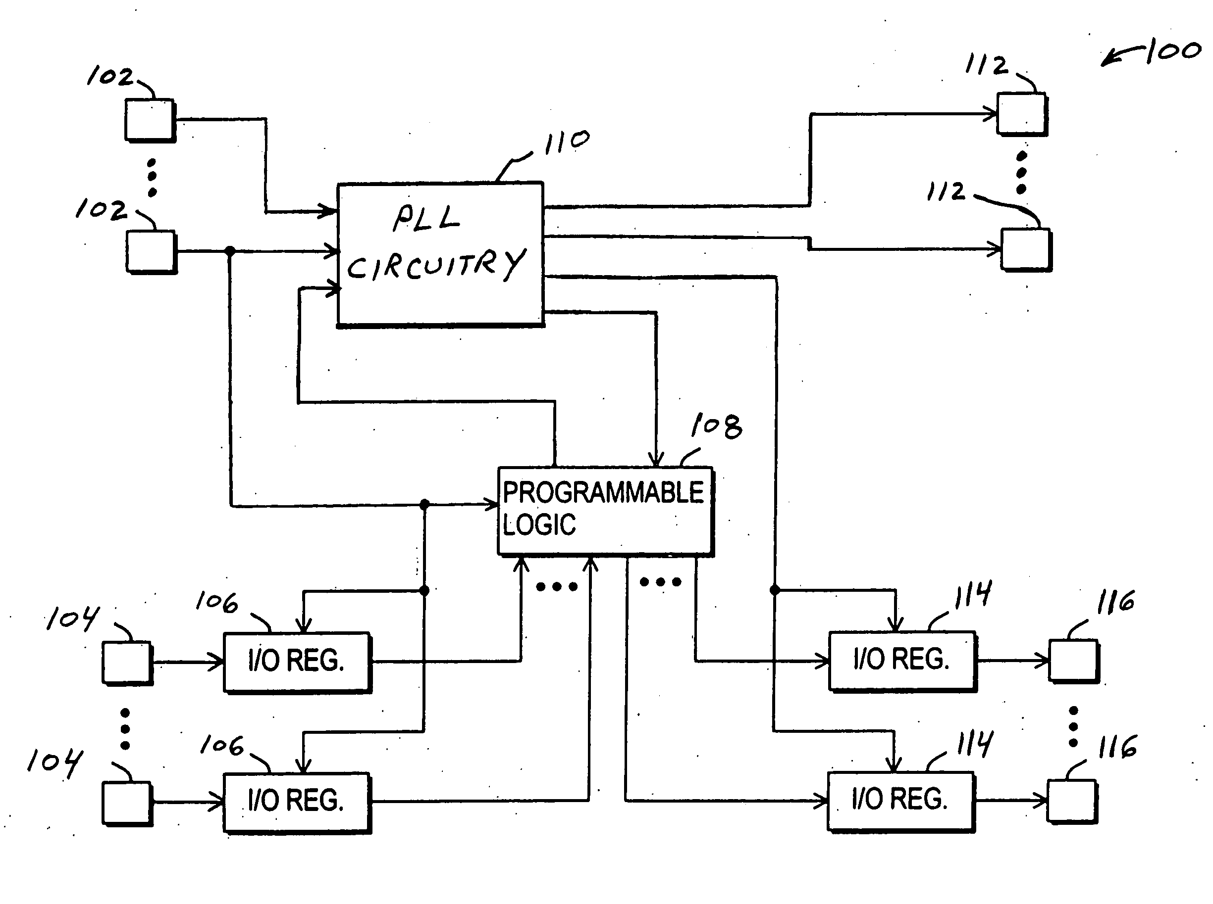
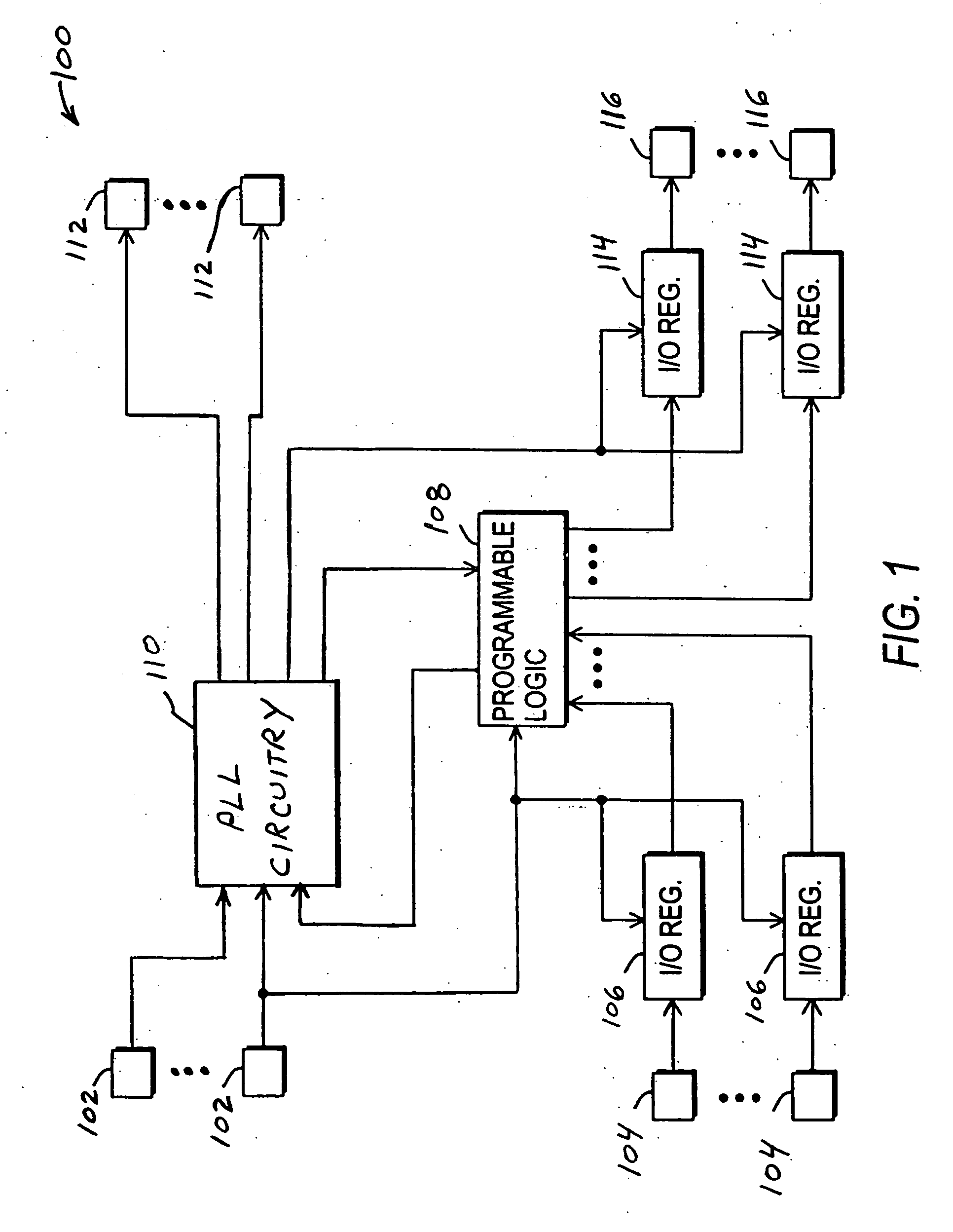
[0025]FIG. 1 shows an illustrative programmable logic integrated circuit device (PLD) 100 in accordance with the invention. PLD 100 has one or more clock signal input pins 102 for receiving one or more clock signals from circuitry external to the device. PLD 100 also includes a plurality of input / output (“I / O”) pins 104 for receiving data and / or control signals from external circuitry. (For convenience herein, all data and control signals other than clock signals will be referred to simply as data signals.) The data signals from pins 104 may be applied to I / O registers 106 for temporary storage and output by those registers. An input clock signal applied to a pin 102 may be applied to I / O registers 106 to control the operation (in particular, the timing) of those registers. The data signals output by registers 106 are applied to programmable logic 108 of PLD 100. (As an alternative to using registers 106, data from pins 104 may be applied more directly to logic 108 (i.e., without fi...


PUM


Abstract

A programmable logic device includes configurable phase-locked loop (PLL) circuitry that outputs multiple clock signals having programmable phases and frequencies. Each output signal is programmably selectable for use as an external clock, internal global clock, internal local clock, or combinations thereof. The PLL circuitry has programmable frequency dividing, including programmable cascaded frequency dividing, and programmable output signal multiplexing that provide a high degree of clock design flexibility.

Description

BACKGROUND OF THE INVENTION [0001] This invention relates to programmable logic integrated circuit devices, and more particularly to configurable phase-locked loop (PLL) circuitry for programmable logic devices. [0002] Programmable logic integrated circuit devices are well known and often include large numbers of programmable logic blocks, memory blocks, and programmable interconnection resources. Logic blocks are programmable by a user to perform various logic functions desired by the user. Memory blocks may be used by the user to store and subsequently output data. Interconnection resources are programmable by the user to make any of a wide range of connections between inputs of the programmable logic device and inputs of the logic and memory blocks, between outputs of the logic and memory blocks and outputs of the device, and between outputs and inputs of the logic and memory blocks. Although each logic block is typically able to perform only a relatively small logic task, such i...

Claims


Application Information

Patent Timeline
15 Sep 2005
Publication
US20050200390A1
IPC
G06F1/06; G06F1/10; G06F1/08; H03K5/13; H03K19/173; H03L7/08; H03L7/081; H03L7/099; H03L7/18; H04J3/06
CPC
H03L7/081; H03L7/18; H03L7/0996
Inventors
STARR, GREGORY W.; CHANG, WANLI