Flash memory device and architecture with multi level cells

a flash memory and multi-level technology, applied in static storage, digital storage, instruments, etc., can solve the problems of reducing the cell state strength of the cell, and reducing the efficiency of flash cell transistors

Active Publication Date: 2005-09-15
SUPER TALENT TECH CORP
View PDF9 Cites 150 Cited by
  • Summary
  • Abstract
  • Description
  • Claims
  • Application Information

AI Technical Summary

Problems solved by technology

This provides a wide noise margin.
Variations in fabrication processes and aging of the device may cause shifts in the threshold of the FLASH cell transistors.
These shifts can weaken the cell state strength by moving the cell closer to the next reference voltage.
While the binary-search comparison of reference voltages to the sensing node is useful, the sequential nature of such comparison introduces more delays as the number of levels per cell increases.

Method used


Image

  • Flash memory device and architecture with multi level cells
  • Flash memory device and architecture with multi level cells
  • Flash memory device and architecture with multi level cells

Examples


Embodiment Construction

[0040] The present invention relates to an improvement in multi-level cells. The following description is presented to enable one of ordinary skill in the art to make and use the invention as provided in the context of a particular application and its requirements. Various modifications to the preferred embodiment will be apparent to those with skill in the art, and the general principles defined herein may be applied to other embodiments. Therefore, the present invention is not intended to be limited to the particular embodiments shown and described, but is to be accorded the widest scope consistent with the principles and novel features herein disclosed.

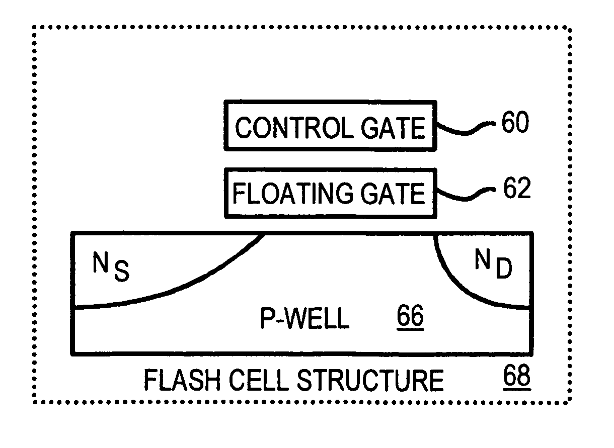
[0041]FIG. 4A shows a FLASH-memory transistor. A FLASH cell can have just transistor 68, or can also have a select transistor in series between the bit line and the drain. Control gate 60 is connected to a word (row) line, while floating gate 62 is isolated from all other nodes by insulators such as oxides. A thin tunneling oxide ...


PUM


Abstract

A FLASH memory has an array of FLASH cells that each store N multiple bits of information as charge stored on a floating gate. Reference voltages or currents are generated for each boundary between the 2N states or levels and for an upper limit and a lower limit reference for each state. A selected bit line driven by a selected FLASH cell generates a sense node that is compared to a full range of 3*2N-1 comparators in parallel. The compare results are decoded to determine which state is read from the selected FLASH cell. An in-range signal is activated when the sense node is between the upper and lower limit references. The target programming count or programming pulses is adjusted during calibration to sense in the middle of the upper and lower limit references. Margin between references is adjusted by calibration codes that select currents for summing.

Description

FIELD OF THE INVENTION [0001] This invention relates to semiconductor memories, and more particularly to multi-level memory cells. BACKGROUND OF THE INVENTION [0002] FLASH memory employing electrically-erasable programmable read-only memory (EEPROM) is widely used today. FLASH memory cells use a floating-gate transistor that has an electrically-insulated gate sandwiched between a control gate and a channel in the substrate between a source and a drain. Charge is injected into the floating gate through a thin tunneling oxide between the substrate and the floating gate. Since the floating gate is surrounded by insulators such as oxide, the charge remains on the floating gate after programming or erasure. [0003] FLASH memory based on n-channel transistors are initially erased. The control gate is grounded and the Vpp programming voltage applied to the drain, reversing the electric field across the thin oxide, and causing electrons to tunnel from the floating gate to the drain. Removing...

Claims


Application Information

Patent Timeline
Patent Type & Authority Applications(United States)
IPC IPC(8): G11C11/00
CPCG11C7/1006G11C2211/5634G11C2211/5631G11C11/5642
Inventor CHEN, BEN WEICHANG, AUGUSTINE W.
Owner SUPER TALENT TECH CORP
Why Eureka
Try Eureka