Photoelectric converting film stack type solid-state image pickup device

a technology of photoelectric and solid-state image, which is applied in the direction of electrical equipment, semiconductor devices, radio frequency control devices, etc., can solve the problems of bad production yield, quantity of photoelectric charges accumulated, and ccd-type image sensors or cmos-type image sensors reaching the limit of their technical progress, so as to achieve efficient removal of photoelectric charges

Inactive Publication Date: 2005-09-22
FUJIFILM HLDG CORP +1
View PDF3 Cites 99 Cited by
  • Summary
  • Abstract
  • Description
  • Claims
  • Application Information

AI Technical Summary

Benefits of technology

[0015] An object of the present invention is to provide a photoelectric converting film stack type solid-state image pickup device where when a photoelectric converting film, for example, using a CdSe quantum dot with ZnS shell is used to fabricate the solid-state image pickup device, the photoelectric charges can be efficiently taken out from the photoelectric converting film.
[0017] By virtue of this constitution, the signal charges generated upon entering of light into the quantum dot can be efficiently read out from the photoelectric converting film.
[0019] By virtue of this constitution, the signal charges can be more efficiently taken out from the photoelectric converting film.
[0021] By virtue of this constitution, the signal charges can be more easily read out from the photoelectric converting film.
[0025] By virtue of this constitution, the signal charges can be more easily and efficiently read out from the photoelectric converting film.
[0027] By virtue of this constitution, the electron-hole pair generated upon entering of light is prevented from recombining.

Problems solved by technology

However, CCD-type image sensors or CMOS-type image sensors are reaching the limit of their technical progress and come to encounter a problem of bad production yield because the opening size of one light-receiving part is about 2 μm and approximated to the wavelength order of incident light.
Furthermore, the upper limit of the quantity of photoelectric charges accumulated in one minute light-receiving part is as small as about 3,000 electrons and with this number of electrons, it is difficult to clearly express 256 gradations.
Therefore, CCD-type or CMOS-type image sensors can be hardly expected to be more enhanced in view of pictorial quality or sensitivity.
However, since the ultrafine particle used is silicon in both of Japanese Patent No. 3,405,099 and JP-A-2002-83946, an electron-hole pair generated upon receiving light cannot be satisfactorily prevented from recombining on the ultrafine particle surface and this causes a problem that the performance as a solid-state image pickup device is not satisfied.
In order to practically use the photoelectric converting film stack type solid-state image pickup device, what material is used to form the photoelectric converting film is present as a problem.
However, it is necessary to solve another problem that even when a CdSe quantum dot with an ZnS shell is merely dispersed in a medium and formed into a film and the film (photoelectric converting film) is interposed between upper and lower transparent electrode films and applied with a voltage, the photoelectric charges (signal charges) cannot be efficiently taken out.

Method used


Image

  • Photoelectric converting film stack type solid-state image pickup device
  • Photoelectric converting film stack type solid-state image pickup device
  • Photoelectric converting film stack type solid-state image pickup device

Examples


Embodiment Construction

[0044] One embodiment of the present invention is described below by referring to the drawings.

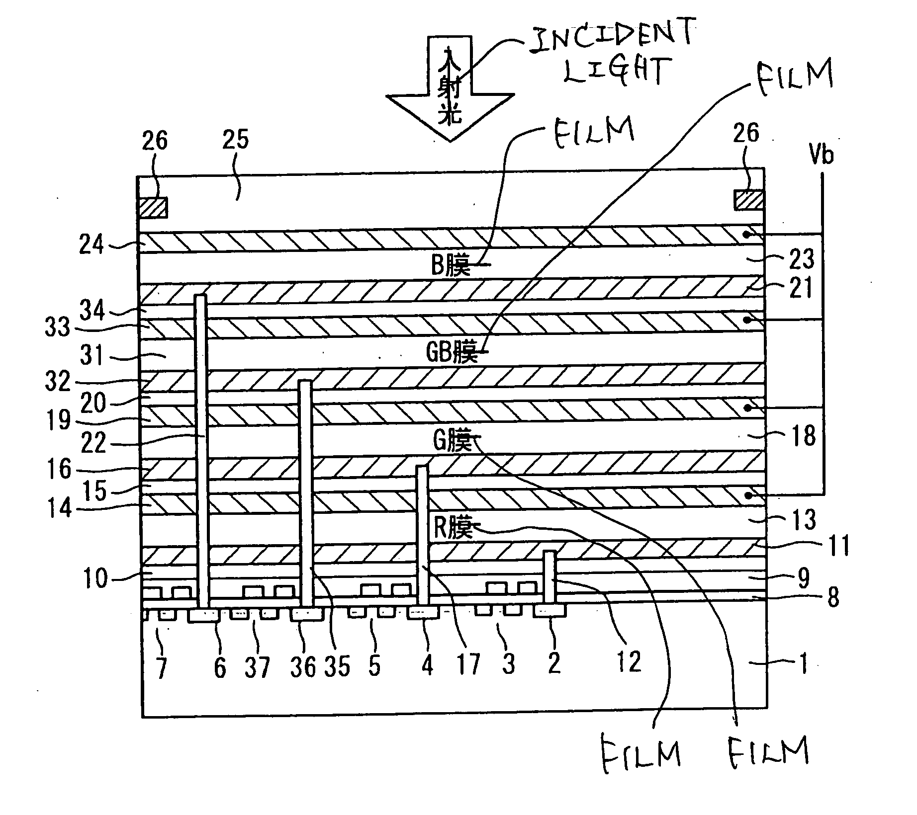
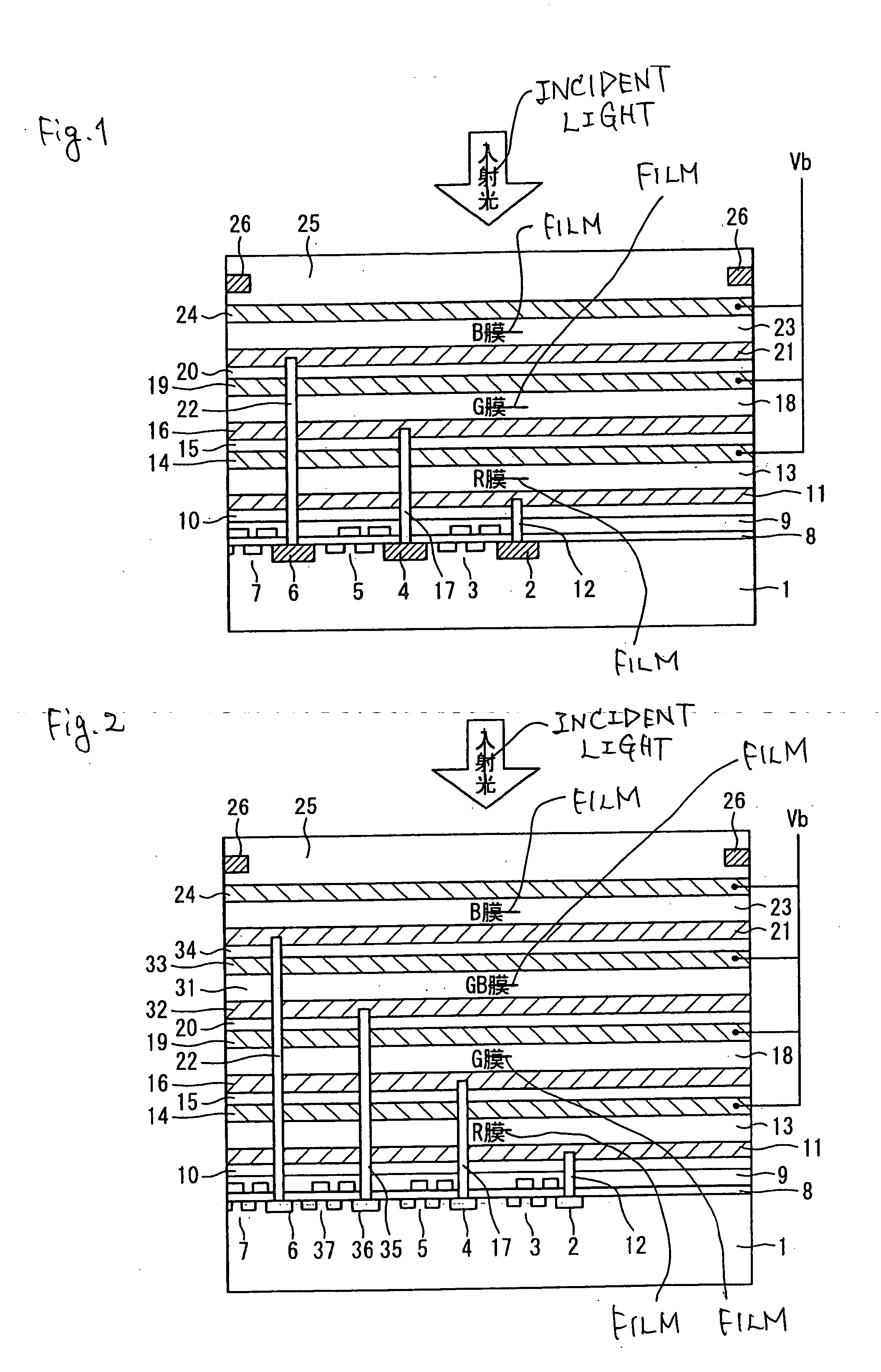
[0045]FIG. 1 is a cross-sectional schematic view of one pixel portion of the photoelectric converting film stack type solid-state image pickup device according to one embodiment of the present invention. This embodiment takes a constitution such that photoelectric converting films are stacked in three layers to take out electrical signals corresponding to three primary colors of red (R), green (G) and blue (B), namely, a constitution of picking up a color image, but a constitution of picking up a monochromatic image, for example, a black-and-white image, by providing only one photoelectric converting film layer may also be employed.

[0046] In FIG. 1, a high-concentration impurity region 2 for accumulating the red color signal, an MOS circuit 3 for reading out the red color signal, a high-concentration impurity region 4 for accumulating the green signal, an MOS circuit 5 for reading out th...


PUM


Abstract

A photoelectric converting film stack type solid-state image pickup device comprising: a semiconductor substrate in which a signal read circuit is formed; and at least one photoelectric converting film interposed between two electrode films, said at least one photoelectric converting film being stacked above the semiconductor substrate, wherein a signal corresponding to an intensity of incident light is read outside by the signal read circuit, the signal being generated by photoelectric conversion with the photoelectric converting film, wherein the photoelectric converting film comprises: a first layer comprising: an ultrafine particle including (i) a quantum dot contributing to the photoelectric conversion and (ii) a material having a band gap larger than that of the quantum dot, the quantum dot being coated with the material; and a hole transport layer stacked on the first layer.

Description

BACKGROUND OF THE INVENTION [0001] 1. Field of the Invention [0002] The present invention relates to a photoelectric converting film stack type solid-state image pickup device fabricated by stacking a photoelectric converting film on a semiconductor substrate having formed on the surface thereof a signal read circuit. [0003] 2. Description of the Related Art [0004] As for the photoelectric converting film stack type solid-state image pickup device, a prototype device is described, for example, in JP-A-58-103165. In this solid-state image pickup device, three photosensitive layers are stacked on a semiconductor substrate, and electrical signals of red (R), green (G) and blue (B) detected by respective photosensitive layers are read out by MOS circuits formed on the semiconductor substrate surface. [0005] Solid-state image pickup devices having such a constitution were proposed in the past and thereafter, CCD-type image sensors or CMOS-type image sensors where a large number of light-...

Claims


Application Information

Patent Timeline
Patent Type & Authority Applications(United States)
IPC IPC(8): H01L27/146H01L27/15
CPCH01L27/14647B82Y10/00
Inventor FUKUNAGA, TOSHIAKI
Owner FUJIFILM HLDG CORP
Why Eureka
Try Eureka