Semiconductor device and manufacturing method thereof

a semiconductor and manufacturing method technology, applied in semiconductor devices, solid-state devices, basic electric elements, etc., can solve the problems of high resistance, increased concentration of impurities, loss, etc., and achieves high-reliability semiconductor devices, efficient removal, and low resistance

Inactive Publication Date: 2015-08-18
SEMICON ENERGY LAB CO LTD
View PDF25 Cites 0 Cited by
  • Summary
  • Abstract
  • Description
  • Claims
  • Application Information

AI Technical Summary

Benefits of technology

[0014]Because the barrier film is provided, Cu does not form an alloy with Si. Thus, the Si film functions as a photoelectric conversion layer and a highly reliable semiconductor device can be obtained.
[0018]In general, a metal film which is formed by sputtering has an average surface roughness (Ra) of about 0.8 nm to 1.5 nm, while a metal plating film has an Ra of about 4 nm. A metal plating film has a more uneven surface than a metal film which is formed by sputtering. Therefore, it is difficult to bond a substrate provided with a metal plating film and a counter substrate to each other. On the other hand, the above-mentioned manufacturing method enables bonding even if a surface has large unevenness.
[0023]A Cu plating film has a lower resistance than an Al film or a sputtered film. With the use of a Cu plating film for an electrode of a photoelectric conversion device such as a solar cell, charges generated by light can be efficiently taken out. In addition, because a barrier film is provided, Cu does not form an alloy with Si and a highly reliable semiconductor device can be obtained. Although a substrate provided with a Cu plating film having a highly uneven surface is used, the substrate and a counter substrate can easily be bonded to each other by thermocompression bonding.

Problems solved by technology

Specific problems are the following: (1) high resistance of a semiconductor device due to the use of an Al electrode, (2) formation of an alloy by Al and Si, (3) high resistance of a film formed by a sputtering method, and (4) defective bonding in a bonding step which is caused if a bonding surface has a large unevenness.
Therefore, the high resistance causes a loss when electromotive force generated in a solar cell is taken out.
In particular, a metal film which is formed by a sputtering method tends to have low electric conductivity.
Although this depends on the element, this is caused by incorporation of a gas used for deposition into a film and an increase in concentration of an impurity in the film.

Method used


Image

  • Semiconductor device and manufacturing method thereof
  • Semiconductor device and manufacturing method thereof
  • Semiconductor device and manufacturing method thereof

Examples


embodiment 1

(Embodiment 1)

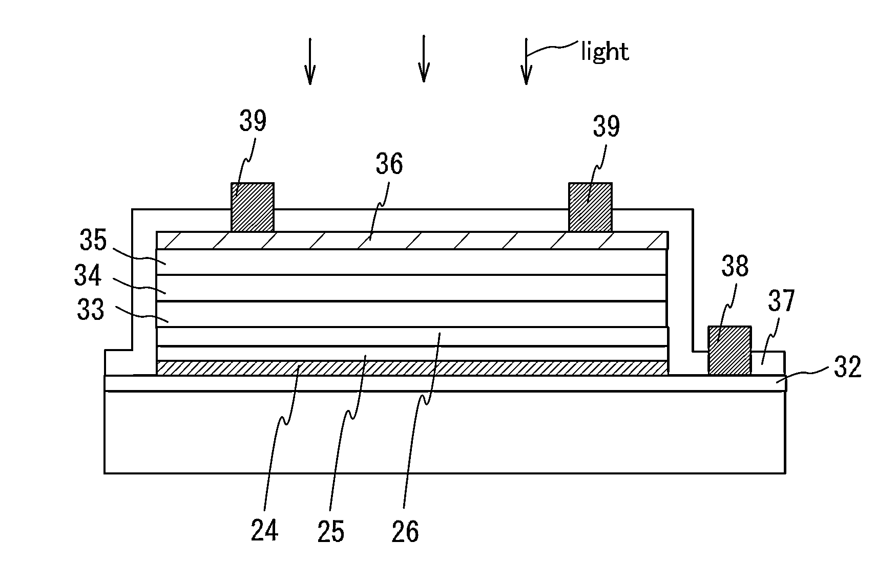
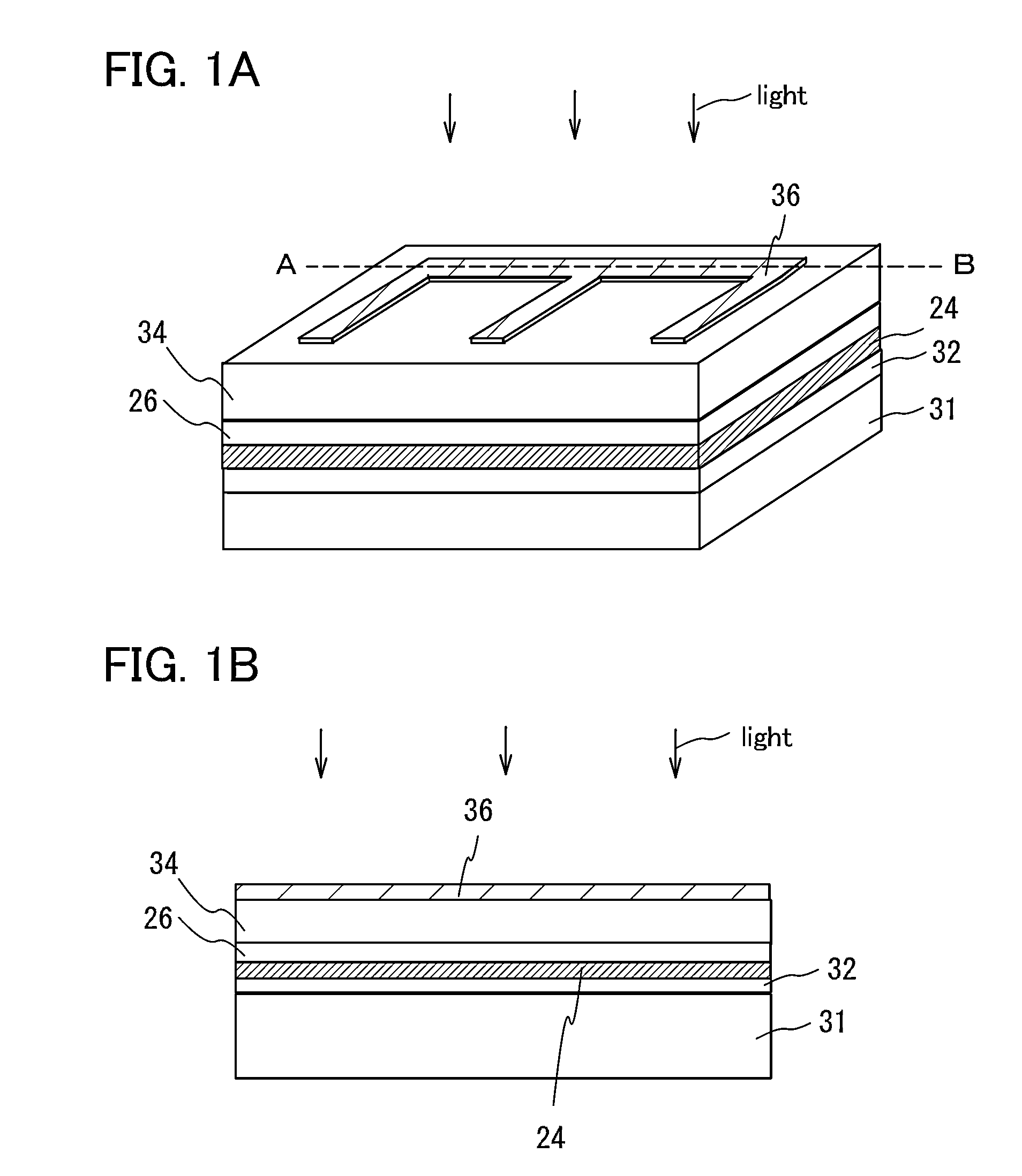
[0038]Embodiment 1 discloses with reference to FIGS. 1A and 1B a semiconductor device including a metal substrate or a substrate provided with a metal film, a copper (Cu) plating film over the metal substrate or the metal film, a barrier film over the Cu plating film, a single crystal silicon film over the barrier film, and an electrode layer over the single crystal silicon film.

[0039]FIG. 1A is a perspective view of a semiconductor device, and FIG. 1B is a cross-sectional view taken along the broken line A-B of FIG. 1A.

[0040]The semiconductor device includes a metal film 32 over a substrate 31, a Cu plating film 24 over the metal film 32, a barrier film 26 over the Cu plating film 24, a single crystal silicon film 34 over the barrier film 26, and an electrode layer 36 over the single crystal silicon film 34.

[0041]The substrate 31 may be, for example, an insulating substrate such as a glass substrate, a quartz substrate, a ceramic substrate, or a plastic substrate, a s...

embodiment 2

(Embodiment 2)

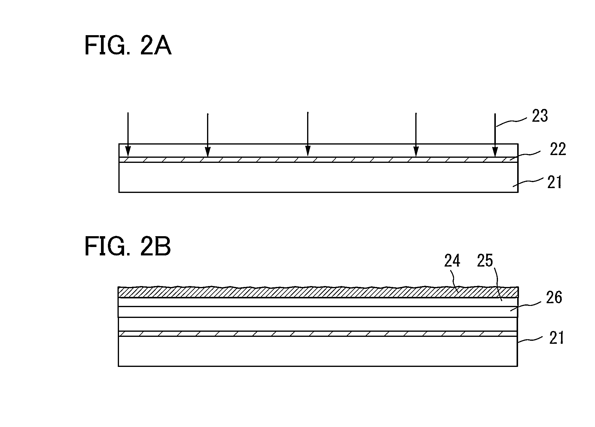
[0050]Embodiment 2 discloses with reference to FIGS. 2A and 2B, FIGS. 3A to 3C, FIGS. 4A to 4C, and FIG. 5 a method for manufacturing a semiconductor device, which includes the steps of: forming an embrittled layer in a single crystal silicon substrate which is a first substrate by doping a surface, preferably an entire surface, of the single crystal silicon substrate with ions which are generated from a hydrogen gas; forming a barrier film over the single crystal silicon substrate; forming a Cu plating film over the barrier film; preparing a second substrate which is a metal substrate or a substrate provided with a metal film; bonding the single crystal silicon substrate and the second substrate to each other with the Cu plating film interposed therebetween or with the Cu plating film and the metal film interposed therebetween by thermocompression bonding of the Cu plating film and the metal substrate or the metal film; forming a single crystal silicon film over the s...

example 1

[0077]Example 1 discloses with reference to FIGS. 6A and 6B, FIGS. 7A and 7B, and FIG. 8 a method for manufacturing a semiconductor device in which a first substrate with a Cu plating film and a second substrate provided with a metal film are bonded to each other with the Cu plating film and the metal film interposed therebetween through thermocompression bonding.

[0078]A Ti film, a titanium nitride film, or a tantalum nitride film having a thickness of 25 nm to 100 nm was formed using a sputtering method as a barrier film 4 over a first substrate 1 which is a single crystal silicon substrate.

[0079]A Ni film, an Ag—Pd—Cu alloy film, or a Cu film having a thickness of 100 nm to 200 nm was formed as a seed film 3 over the barrier film 4 using a sputtering method (FIG. 6A).

[0080]A Cu plating film was formed over the seed film 3. The formation of the Cu plating film includes pretreatment, plating treatment, and post-treatment.

[0081]The pretreatment is described. The first substrate 1 pro...


PUM

PropertyMeasurementUnit
thicknessaaaaaaaaaa
resistivityaaaaaaaaaa
Raaaaaaaaaaa

Abstract

An object relates to an electrode of a semiconductor device or a method for manufacturing a semiconductor device, which includes a bonding step, and problems are: (1) high resistance of a semiconductor device due to the use of an Al electrode, (2) formation of an alloy by Al and Si, (3) high resistance of a film formed by a sputtering method, and (4) defective bonding in a bonding step which is caused if a bonding surface has a large unevenness. A semiconductor device includes a metal substrate or a substrate provided with a metal film, a copper (Cu) plating film over and bonded to the metal substrate or the metal film by employing a thermocompression bonding method, a barrier film over the Cu plating film, a single crystal silicon film over the barrier film, and an electrode layer over the single crystal silicon film.

Description

BACKGROUND OF THE INVENTION[0001]1. Field of the Invention[0002]The present invention relates to semiconductor devices such as photoelectric conversion devices including solar cells and a manufacturing method thereof.[0003]2. Description of the Related Art[0004]Patent Document 1 discloses a method for manufacturing a solar cell, in which a silicon (Si) film is formed over a substrate by bonding a silicon wafer to the substrate and separating the silicon film from the silicon wafer.[0005]The method for manufacturing a solar cell, which is disclosed in FIGS. 10A to 10D of Patent Document 1, is as follows. A bonding metal layer such as an evaporated aluminum (Al) layer is formed over a silicon wafer in which hydrogen has been implanted. The bonding metal layer and an Al-based metal substrate are disposed in close contact with each other. A part of the silicon wafer is separated by heat treatment at 400° C. to 600° C., whereby a silicon film is formed over the Al-based metal substrate w...

Claims


Application Information

Patent Timeline
Patent Type & Authority Patents(United States)
IPC IPC(8): H01L31/0224H01L31/0296H01L31/02H01L31/028H01L31/068H01L31/075
CPCH01L31/022425H01L31/0296H01L31/028H01L31/02008H01L31/068H01L31/075Y02E10/50Y02E10/547Y02E10/548H01L21/3223H01L27/12H01L31/0392H01L31/04
Inventor FUJII, TERUYUKIOHSHIMA, KOHEIMARUYAMA, JUNYASHIMOMURA, AKIHISA
Owner SEMICON ENERGY LAB CO LTD
Why Eureka
Try Eureka