Method for using sputtering target and method for manufacturing oxide film

Inactive Publication Date: 2014-01-02
SEMICON ENERGY LAB CO LTD
View PDF4 Cites 27 Cited by
  • Summary
  • Abstract
  • Description
  • Claims
  • Application Information

AI Technical Summary

Benefits of technology

[0103]It is possible to provide a transistor which has stable electrical characteristics with the use of an oxide film with a high degr

Problems solved by technology

Although an oxide semiconductor containing a plurality of metal elements has high controllability of carrier density, th

Method used


Image

  • Method for using sputtering target and method for manufacturing oxide film
  • Method for using sputtering target and method for manufacturing oxide film
  • Method for using sputtering target and method for manufacturing oxide film

Examples


embodiment 1

[0142]In this embodiment, a method for using a sputtering target including a polycrystalline oxide is described.

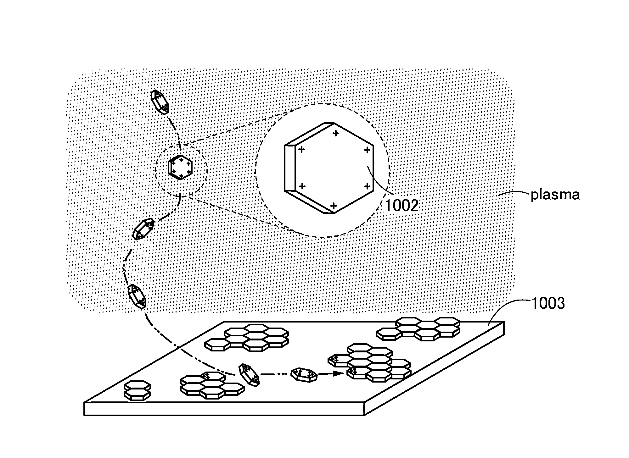
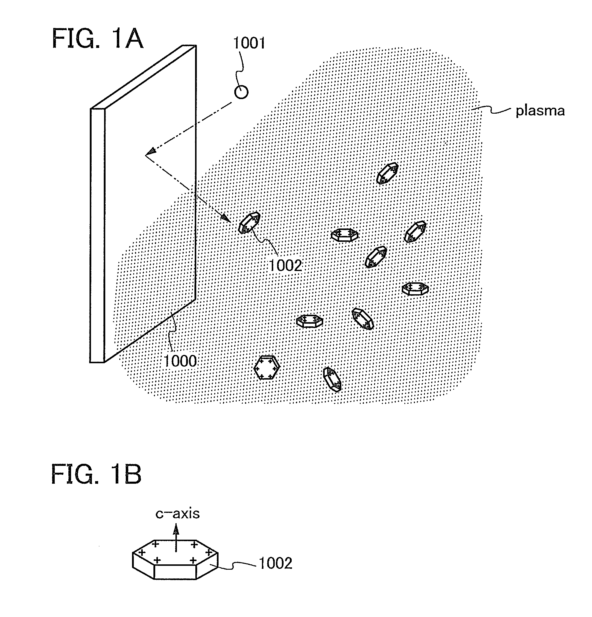
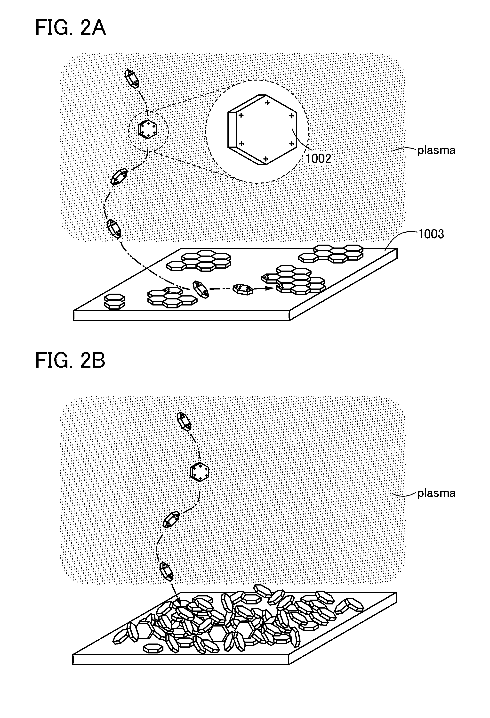
[0143]FIG. 1A is a schematic diagram illustrating a state in which an ion 1001 collides with a sputtering target 1000 to separate sputtered particles 1002 from the sputtering target 1000. Note that the sputtered particle 1002 may have the shape of a hexagonal cylinder whose hexagonal planes are parallel to an a-b plane. In that case, the direction perpendicular to the hexagonal planes is a c-axis direction (see FIG. 1B). The diameter of the plane of the sputtered particle 1002, which is parallel to the a-b plane, is approximately greater than or equal to 1 nm and less than or equal to 30 nm or greater than or equal to 1 nm and less than or equal to 10 nm, though it differs depending on the kind of oxide. Note that an oxygen cation is used as the ion 1001. An argon cation may be used in addition to the oxygen cation. Note that a cation of another rare gas may be used instea...

embodiment 2

[0157]In this embodiment, a film formation apparatus for forming the oxide film with a high degree of crystallinity described in Embodiment 1 is described.

[0158]First, a structure of a film formation apparatus which allows the entry of few impurities into a film during film formation is described with reference to FIG. 12 and FIGS. 13A to 13C.

[0159]FIG. 12 is a top view schematically illustrating a single wafer multi-chamber film formation apparatus 4000. The film formation apparatus 4000 includes an atmosphere-side substrate supply chamber 4001 including a cassette port 4101 for holding a substrate and an alignment port 4102 for performing alignment of a substrate, an atmosphere-side substrate transfer chamber 4002 through which a substrate is transferred from the atmosphere-side substrate supply chamber 4001, a load lock chamber 4003a where a substrate is carried and the pressure inside the chamber is switched from an atmospheric pressure to a reduced pressure or from a reduced pr...

embodiment 3

[0229]In this embodiment, a sputtering target of one embodiment of the present invention is described.

[0230]A sputtering target is a sputtering target where impurity concentration is reduced. Specifically, the concentration of silicon in the sputtering target is set to be lower than 1×10¹⁹ atoms / cm3, preferably lower than 5×10¹⁸ atoms / cm3, more preferably lower than 1×10¹⁸ atoms / cm3. The concentration of carbon in the sputtering target is set to be lower than 1×10¹⁹ atoms / cm3, preferably lower than 5×10¹⁸ atoms / cm3, more preferably lower than 1×10¹⁸ atoms / cm3. The concentration of iron in the sputtering target is set to be lower than 1×10¹⁶ atoms / cm3, preferably lower than 5×10¹⁵ atoms / cm3, more preferably lower than 1×10¹⁵ atoms / cm3. The concentration of nickel in the sputtering target is set to be lower than 5×10¹⁶ atoms / cm3, preferably lower than 1×10¹⁶ atoms / cm3, more preferably lower than 5×10¹⁵ atoms / cm3, further preferably lower than 1×10¹⁵ atoms / cm3. It is preferable to use ...


PUM

PropertyMeasurementUnit
Crystallinityaaaaaaaaaa
Shapeaaaaaaaaaa

Abstract

A method for using a sputtering target which enables an oxide film with a high degree of crystallinity, which contains a plurality of metal elements, to be formed is provided. In the method for using a sputtering target including a polycrystalline oxide containing a plurality of crystal grains which include a cleavage plane, an ion is made to collide with the sputtering target to separate sputtered particles from the cleavage plane, and the sputtered particles are positively charged, so that the sputtered particles are deposited uniformly on a deposition surface while repelling each other.

Description

TECHNICAL FIELD[0001]The present invention relates to an object, a method, or a manufacturing method. In addition, the present invention relates to a process, a machine, manufacture, or a composition of matter. In particular, the present invention relates to, for example, a semiconductor device, a display device, a light-emitting device, a power storage device, a driving method thereof, or a manufacturing method thereof. The present invention particularly relates to a semiconductor device, a display device, or a light-emitting device each including an oxide semiconductor, for example. The present invention further particularly relates to a sputtering target and a manufacturing method thereof, for example. Alternatively, the present invention relates to an oxide film formed by a sputtering method, using the sputtering target, and a semiconductor device including the oxide film, for example.[0002]In this specification, a semiconductor device generally refers to a device which can func...

Claims


Application Information

Patent Timeline
IPC IPC(8): C23C14/34H05B44/00
CPCC23C14/34C23C14/08C23C14/086C23C14/3414C23C14/564H01L29/513H01L29/517H01L29/7869C23C14/352C23C14/3464
Inventor YAMAZAKI, SHUNPEI
Owner SEMICON ENERGY LAB CO LTD
Why Eureka
Try Eureka