Semiconductor device and method for manufacturing the same

a semiconductor device and semiconductor technology, applied in the field of semiconductor devices, can solve the problems of difficult to increase the area of the soi substrate, and achieve the effects of reducing the reliability increasing the area of the semiconductor device, and improving productivity

Inactive Publication Date: 2009-03-26
SEMICON ENERGY LAB CO LTD
View PDF23 Cites 29 Cited by
  • Summary
  • Abstract
  • Description
  • Claims
  • Application Information

AI Technical Summary

Benefits of technology

[0019]According to the present invention, a large-area semiconductor substrate (SOI substrate) can be provided. That is, an area of a semiconductor device can be increased. Thus, the productivity can be improved. Furthermore, even in the case where a substrate including a

Problems solved by technology

Therefore, it has been difficult to i

Method used


Image

  • Semiconductor device and method for manufacturing the same
  • Semiconductor device and method for manufacturing the same
  • Semiconductor device and method for manufacturing the same

Examples


embodiment mode 1

[0048]This embodiment mode describes a semiconductor substrate having a plurality of single crystal semiconductor layers over a substrate, and a method for manufacturing the semiconductor substrate.

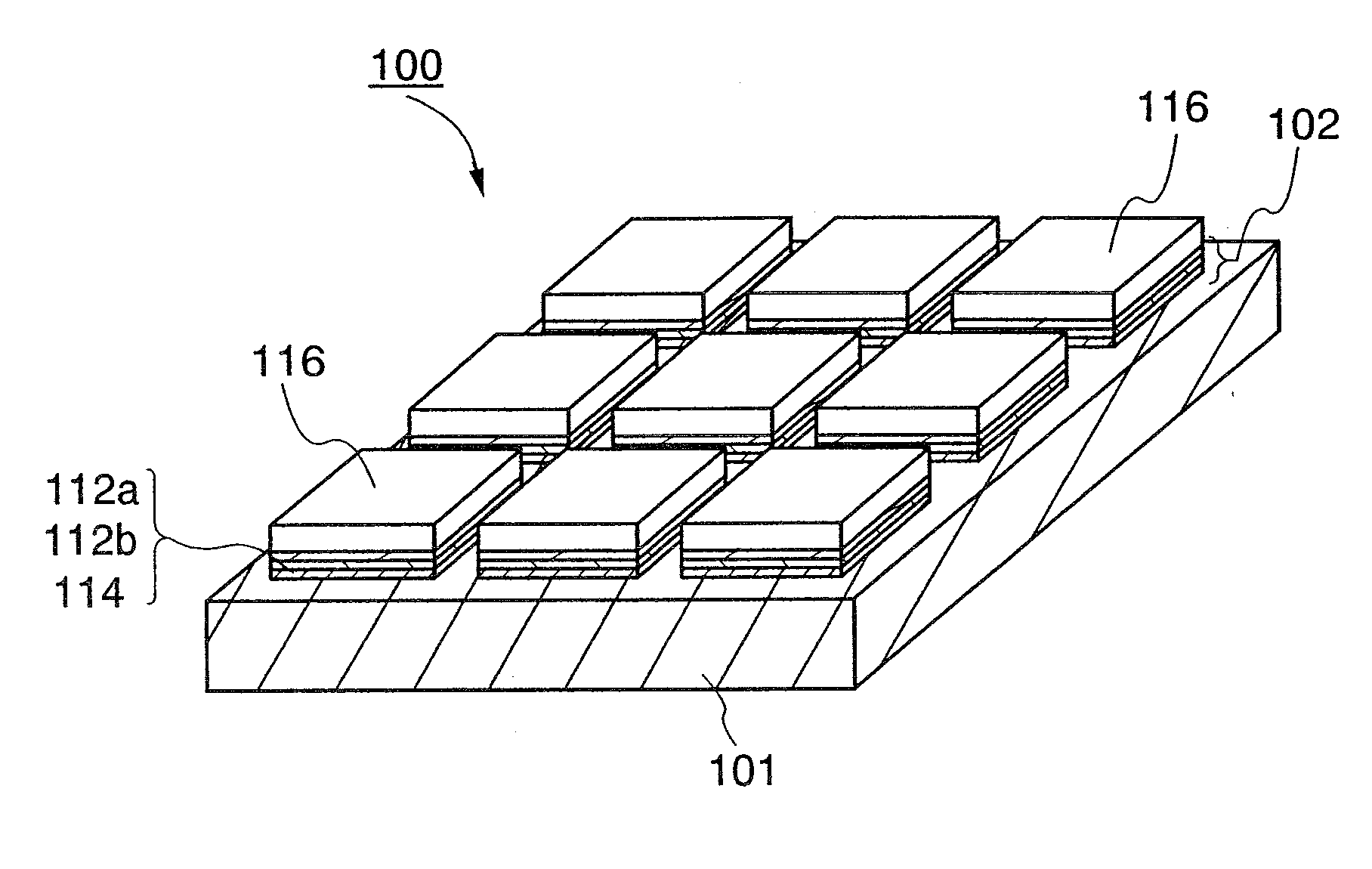
[0049]FIG. 1 is a perspective view showing a structural example of a semiconductor substrate 100. The semiconductor substrate 100 has a structure in which a plurality of single crystal semiconductor layers 116 are bonded to one base substrate, which is a base substrate 101. Each of the single crystal semiconductor layers 116 is provided for the base substrate 101 with an insulating layer 102 interposed therebetween. The semiconductor substrate 100 is a so-called SOI substrate.

[0050]The insulating layer 102 may have a single-layer structure or a stacked-layer structure. In this embodiment mode, the insulating layer 102 has a three-layer structure, in which a bonding layer 114, an insulating film 112b (a silicon nitride oxide layer), and an insulating film 112a (a silicon oxynitride layer) ...

embodiment mode 2

[0126]This embodiment mode describes reprocessing of a single crystal semiconductor substrate. In specific, the case where the single crystal semiconductor substrates 117 shown in FIG. 8B is reprocessed is described with reference to FIGS. 11A to 11D.

[0127]After the process of FIG. 8B, a projection 117a is formed in the periphery of the single crystal semiconductor substrate 117 as shown in FIGS. 11A to 11D, and an insulating film 112a, an insulating film 112b, and a bonding layer 114 are left over the projection 117a.

[0128]First, etching treatment by which the insulating film 112a, the insulating film 112b, and the bonding layer 114 are removed is performed. When these films and the layer are formed from silicon oxide, silicon oxynitride, or silicon nitride oxide, wet etching treatment using hydrofluoric acid may be performed, for example. By the etching treatment, a single crystal semiconductor substrate 117 as shown in FIG. 11B is obtained. FIG. 11C is a cross-sectional view tak...

embodiment mode 3

[0134]This embodiment mode describes, with reference to FIGS. 12A to 12C, the case where an insulating layer serving as a barrier layer is provided over a base substrate, as another example of a semiconductor substrate having a plurality of single crystal semiconductor layers over a substrate. Note that for most part of a method for manufacturing a semiconductor substrate of this embodiment mode, Embodiment Mode 1 can be referred to.

[0135]FIG. 12A is a perspective view showing a structural example of a semiconductor substrate 100. FIG. 12B is a cross-sectional view of FIG. 12A. The semiconductor substrate 100 has a structure in which a plurality of single crystal semiconductor layers 116 are bonded to one base substrate, which is a base substrate 101. Each of the single crystal semiconductor layers 116 is provided over the base substrate 101 with an insulating layer 102 and an insulating layer 103 interposed therebetween, and the semiconductor substrate 100 is referred to as a so-ca...


PUM


Abstract

To provide a method for manufacturing a large-area semiconductor device, to provide a method for manufacturing a semiconductor device with high efficiency, and to provide a highly-reliable semiconductor device in the case of using a large-area substrate including an impurity element. A plurality of single crystal semiconductor substrates are concurrently processed to manufacture an SOI substrate, so that an area of a semiconductor device can be increased and a semiconductor device can be manufactured with improved efficiency. In specific, a series of processes is performed using a tray with which a plurality of semiconductor substrates can be concurrently processed. Here, the tray is provided with at least one depression for holding single crystal semiconductor substrates. Further, deterioration of characteristics of a manufactured semiconductor element is prevented by providing an insulating layer serving as a barrier layer against an impurity element which may affect characteristics of the semiconductor element.

Description

BACKGROUND OF THE INVENTION[0001]1. Field of the Invention[0002]The present invention relates to a semiconductor device having an SOI (silicon on insulator) structure and a method for manufacturing the semiconductor device. In this specification, the semiconductor device refers to any device which can function with the use of semiconductor characteristics.[0003]2. Description of the Related Art[0004]In recent years, VLSI technology has been dramatically progressed, and an SOI structure by which speeding up and low power consumption are realized has been attracted attention. In this technology, an active region (channel formation region) of a field-effect transistor (FET), which has been conventionally formed using bulk single crystal silicon, is formed using a single crystal silicon thin film. It is known that a MOS field-effect transistor manufactured using an SOI structure has lower parasitic capacitance than that manufactured using a conventional bulk single crystal silicon subst...

Claims


Application Information

Patent Timeline
IPC IPC(8): H01L29/00H01L21/762
CPCH01L27/1214H01L27/1266H01L29/66772H01L2924/0002H01L2924/00
Inventor YAMAZAKI, SHUNPEI
Owner SEMICON ENERGY LAB CO LTD
Why Eureka
Try Eureka