Method for manufacturing semiconductor device

a semiconductor and manufacturing technology, applied in vacuum evaporation coatings, transistors, coatings, etc., can solve the problems of increased oxygen vacancies, poor electrical characteristics, increased leakage current, etc., and achieves high reliability of semiconductor devices, suppressed oxygen vacancies in oxide semiconductor layers, and favorable electrical characteristics

Active Publication Date: 2015-10-06
SEMICON ENERGY LAB CO LTD
View PDF149 Cites 31 Cited by
  • Summary
  • Abstract
  • Description
  • Claims
  • Application Information

AI Technical Summary

Benefits of technology

[0009]Thus, an object of one embodiment of the present invention is to provide a semiconductor device in which an increase in oxygen vacancies in an oxide semiconductor layer can be suppressed. Another object is to provide a semiconductor device with favorable electrical characteristics. In addition, another object is to provide a highly reliable semiconductor device.
[0020]In one embodiment of the present invention, a semiconductor device in which an increase in oxygen vacancies in an oxide semiconductor layer is suppressed can be provided. Further, a semiconductor device with favorable electrical characteristics can be provided. Further, a highly reliable semiconductor device can be provided.

Problems solved by technology

However, even when an oxide semiconductor layer includes few oxygen vacancies initially, oxygen vacancies will increase in number from various causes.
An increase in oxygen vacancies in an oxide semiconductor layer causes poor electrical characteristics in some cases; for example, the transistor becomes normally-on, leakage current increases, or threshold voltage is shifted due to stress application.

Method used


Image

  • Method for manufacturing semiconductor device
  • Method for manufacturing semiconductor device
  • Method for manufacturing semiconductor device

Examples


embodiment 1

[0046]In this embodiment, a semiconductor device which is one embodiment of the present invention is described with reference to drawings.

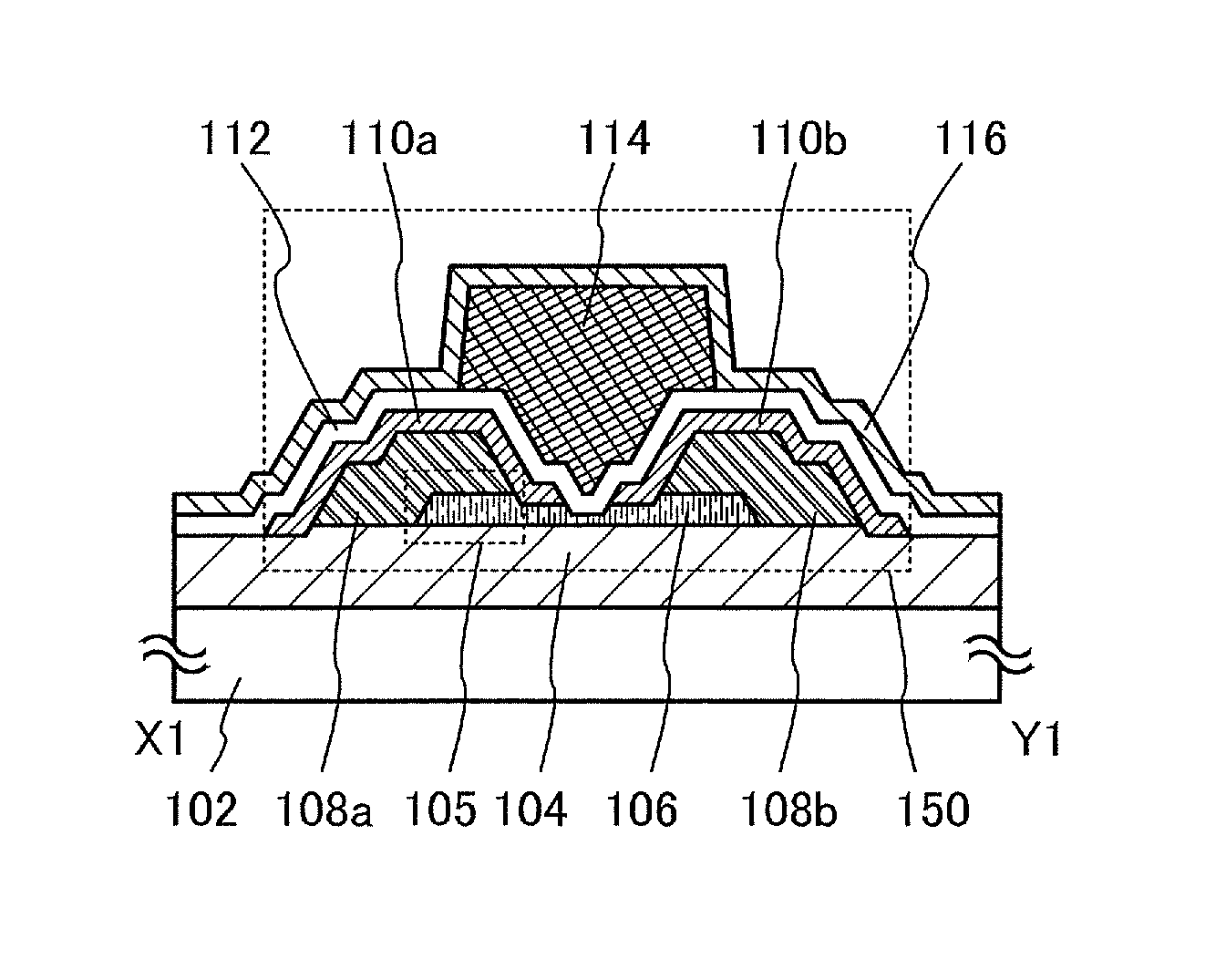
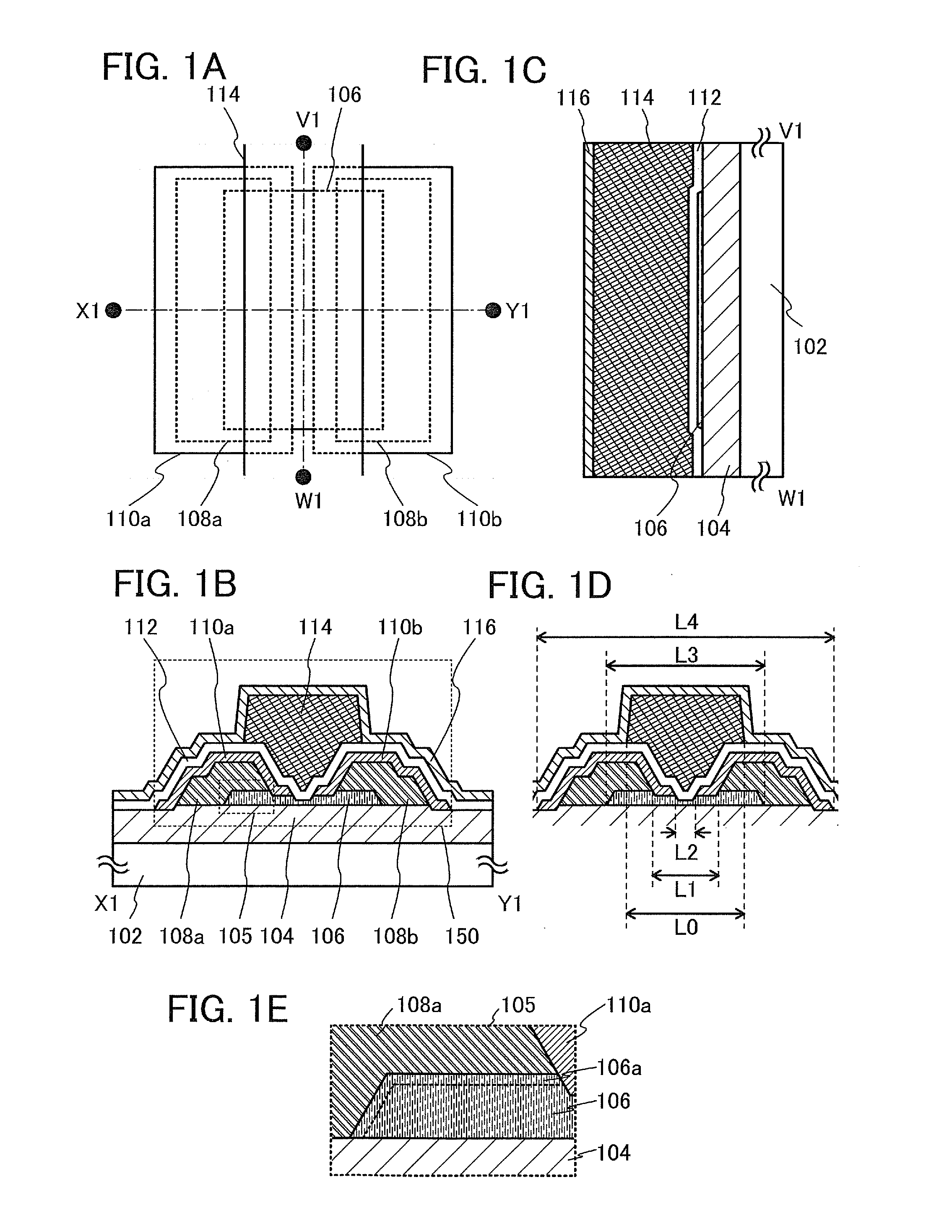
[0047]FIGS. 1A, 1B, 1C, 1D, and 1E are a top view and cross-sectional views which illustrate a transistor of one embodiment of the present invention. FIG. 1A is the top view of the transistor, and a cross section taken along a dashed-dotted line X1-Y1 in FIG. 1A is illustrated in FIG. 1B. A cross section taken along a dashed-dotted line V1-W1 in FIG. 1A is illustrated in FIG. 1C. FIG. 1D illustrates widths of components of the transistor which are illustrated in FIG. 1B. FIG. 1E is an enlarged view of a region 105 illustrated in FIG. 1B. Note that for simplification of the drawing, some components in the top view in FIG. 1A are illustrated in a see-through manner or not illustrated.

[0048]A transistor 150 illustrated in FIGS. 1A, 1B, 1C, 1D, and 1E includes an oxide insulating film 104 formed over a substrate 102; an oxide semiconductor layer 106 f...

embodiment 2

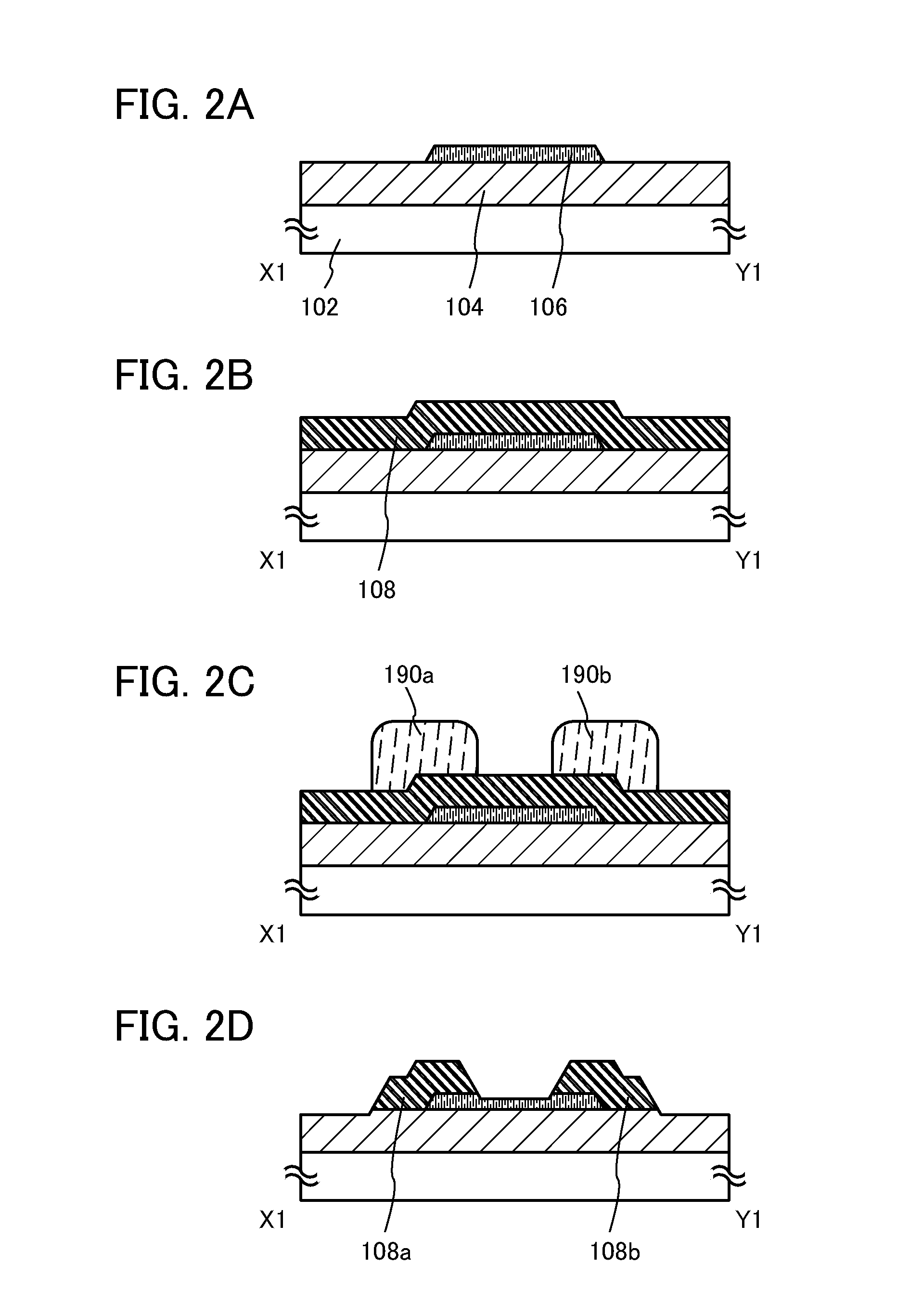
[0086]In this embodiment, a method for manufacturing the transistor 150 described in Embodiment 1 with reference to FIGS. 1A to 1E will be described with reference to FIGS. 2A to 2D, FIGS. 3A to 3D, and FIGS. 4A to 4C.

[0087]For the substrate 102, a glass substrate, a ceramic substrate, a quartz substrate, a sapphire substrate, or the like can be used. Alternatively, a single crystal semiconductor substrate or a polycrystalline semiconductor substrate made of silicon, silicon carbide, or the like, a compound semiconductor substrate made of silicon germanium or the like, a silicon-on-insulator (SOI) substrate, or the like may be used. Still alternatively, any of these substrates further provided with a semiconductor element may be used.

[0088]The oxide insulating film 104 can be formed by a plasma chemical vapor deposition (CVD) method, a sputtering method, or the like using an oxide insulating film of aluminum oxide, magnesium oxide, silicon oxide, silicon oxynitride, silicon nitride ...

embodiment 3

[0136]In this embodiment, a transistor having a structure different from that of the transistor described in Embodiment 1 will be described with reference to FIGS. 5A to 5C and FIGS. 6A to 6D.

[0137]FIGS. 5A, 5B, and 5C are a top view and cross-sectional views which illustrate a transistor of one embodiment of the present invention. FIG. 5A is the top view of the transistor, and a cross section taken along a dashed-dotted line X2-Y2 in FIG. 5A is illustrated in FIG. 5B. A cross section taken along a dashed-dotted line V2-W2 in FIG. 5A is illustrated in FIG. 5C. Note that for simplification of the drawing, some components in the top view in FIG. 5A are illustrated in a see-through manner or not illustrated. Note that the same portions as or portions having functions similar to those of the transistor described in Embodiment 1 are denoted by the same reference numerals, and repeated description thereof is omitted.

[0138]A transistor 152 illustrated in FIGS. 5A, 5B, and 5C includes the o...


PUM

PropertyMeasurementUnit
distanceaaaaaaaaaa
distanceaaaaaaaaaa
distanceaaaaaaaaaa

Abstract

In a semiconductor device in which a channel formation region is included in an oxide semiconductor layer, an oxide insulating film below and in contact with the oxide semiconductor layer and a gate insulating film over and in contact with the oxide semiconductor layer are used to supply oxygen of the gate insulating film, which is introduced by an ion implantation method, to the oxide semiconductor layer.

Description

BACKGROUND OF THE INVENTION[0001]1. Field of the Invention[0002]The present invention relates to a semiconductor device including an oxide semiconductor and a method for manufacturing the semiconductor device.[0003]In this specification, a “semiconductor device” refers to a device that can function by utilizing semiconductor characteristics; an electro-optical device, a semiconductor circuit, and an electric device are all included in the category of the semiconductor device.[0004]2. Description of the Related Art[0005]Attention has been focused on a technique for forming a transistor using a semiconductor thin film formed over a substrate having an insulating surface (also referred to as a thin film transistor (TFT)). The transistor is applied to a wide range of electronic devices such as an integrated circuit (IC) or an image display device (display device). A silicon-based semiconductor material is widely known as a material for a semiconductor thin film applicable to a transisto...

Claims


Application Information

Patent Timeline
Patent Type & Authority Patents(United States)
IPC IPC(8): H01L21/00H01L21/02H01L29/04H01L29/26H01L29/78C23C14/08C23C14/34H01L29/45H01L29/49H01L29/66H01L29/786
CPCH01L21/02565C23C14/086C23C14/3414H01L21/02554H01L21/02592H01L21/02609H01L21/02617H01L21/02631H01L29/045H01L29/26H01L29/45H01L29/4908H01L29/66969H01L29/78H01L29/7869H01L21/02488H01L21/441H01L21/47576H01L21/47635
Inventor YAMAZAKI, SHUNPEISUZAWA, HIDEOMISASAGAWA, SHINYATANAKA, TETSUHIRO
Owner SEMICON ENERGY LAB CO LTD
Why Eureka
Try Eureka