Optical waveguide and the method of fabricating the same

a technology of optical waveguides and optical waveguides, applied in the field of optical waveguides, can solve problems such as reducing the curing

Inactive Publication Date: 2005-09-22
SANYO ELECTRIC CO LTD
View PDF6 Cites 21 Cited by
  • Summary
  • Abstract
  • Description
  • Claims
  • Application Information

AI Technical Summary

Benefits of technology

[0009] It is an object of the present invention to provide an optical waveguide and a method of fabricating the optical waveguide, which can form a clad layer and / or a core layer in such a way that the refractive index of the layer is uniform without being affected by a thickness of a substrate and the like.
[0011] By proving the ultraviolet control region according to the present invention, it is possible to inhibit the ultraviolet light from entering a layer below the ultraviolet control region when the ultraviolet light is irradiated in order to cure resin. Therefore, it is possible to inhibit the ultraviolet light from entering a substrate existing below the ultraviolet control region, for example, by proving the ultraviolet control region on the underside of the lower clad layer. Thus, it is possible to reduce an effect of curing due to the ultraviolet light reflected at the underside of the substrate, which has been a problem. Accordingly, it is possible to inhibit the ultraviolet light reflected at the underside of the substrate from entering the lower clad layer in curing the lower clad layer by irradiating the ultraviolet light and the lower clad layer can be cured in such a way that its refractive index is uniform without being affected by the thickness of the substrate and the like. Further, since an amount of the ultraviolet light passing through the lower clad layer and reflected at the underside of the substrate can be suppressed also in curing the upper clad layer or the core layer, the upper clad layer or the core layer can be cured in such a way that the refractive indexes of these layer are uniform without being affected by the thickness of the substrate and the like.
[0013] When using an upper substrate, the upper clad layer, the core layer and the lower clad layer are formed one by one on the upper substrate, by proving the ultraviolet control region on the upper clad layer, an amount of the ultraviolet light reflected at the topside of the upper substrate can be suppressed in curing the upper clad layer by irradiating the ultraviolet light to it, and therefore the upper clad layer can be cured in such a way that its refractive index is uniform. Similarly, when forming the lower clad layer, the lower clad layer can be formed in such a way that the refractive index of the lower clad layer is uniform since an amount of the ultraviolet light passing through the upper clad layer and reflected at the topside of the upper substrate can be suppressed. Also, when forming the core layer, the core layer can be similarly formed in such a way that its refractive index is uniform. Further, when it is difficult to form the ultraviolet control region on a base, a part of the upper clad layer, the core layer and the lower clad layer may be cured with heat to the extent that temperature does not thermally damaging a layer to be a substrate or a base to form an ultraviolet control region. Specifically, a part of the upper clad layer, the core layer and the lower clad layer can be cured by heating when temperature is below a glass transition point of the layer to be a substrate or a base.
[0014] In the present invention, recesses and projections are preferably formed on the face of at least one side of the ultraviolet control region. By forming such the recesses and projections, it is possible to scatter the ultraviolet light more efficiently on the surface of the ultraviolet control region and inhibit the ultraviolet light from entering. By forming such the recesses and projections, it is possible to scatter the ultraviolet light efficiently even when a difference between two refractive indexes at an interface of the ultraviolet control region and another layer is 0.01 or less. Preferably, the recesses and projections have the surface roughness Rz per a length of 250 μm (JIS B0601) of 50 nm or larger, more preferably 100 nm or larger, and furthermore preferably 400 nm or larger.
[0041] In accordance with the present invention, the clad layer and / or the core layer can be formed in such a way that the refractive index of the layer is uniform without being affected by the thickness of the substrate and the like. Therefore, when the optical waveguide of the present invention is applied for devices for optical communication, variations in insertion loss can be reduced.

Problems solved by technology

Thus, it is possible to reduce an effect of curing due to the ultraviolet light reflected at the underside of the substrate, which has been a problem.

Method used


Image

  • Optical waveguide and the method of fabricating the same
  • Optical waveguide and the method of fabricating the same
  • Optical waveguide and the method of fabricating the same

Examples


example 1

[Measurement of a Refractive Index]

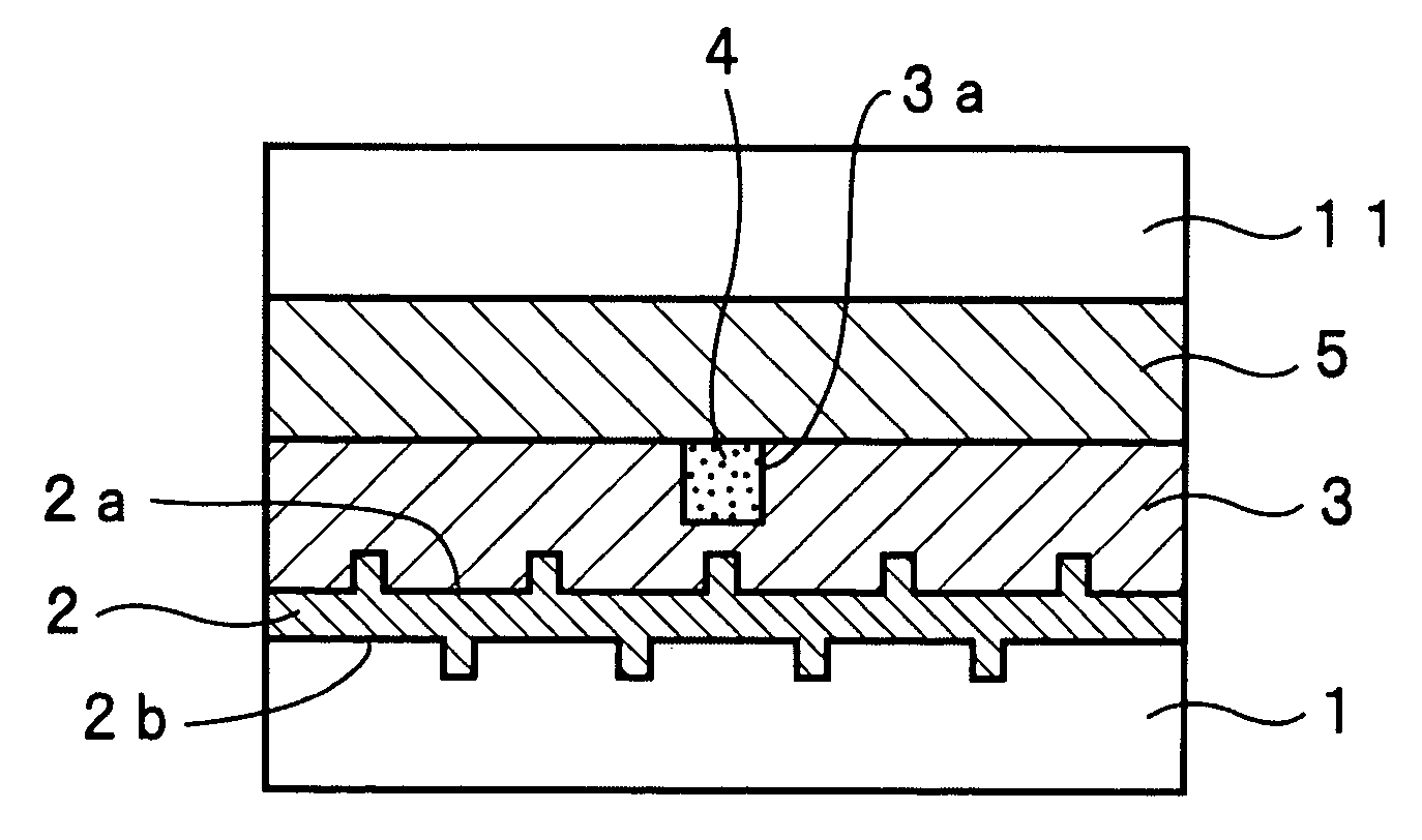
[0113] In order to evaluate the effects of providing the ultraviolet control region 2 on the control of refractive index in the lower clad layer 3 in the embodiment shown in FIG. 1, an ultraviolet control region 2 was formed on each substrate 1 using substrates 1 having different thicknesses, and a lower clad layer 3 was formed on the ultraviolet control region 2, and a refractive index of the lower clad layer 3 was measured in the embodiment shown in FIG. 1. Specifically, substrates having a thickness of 0.5 mm, 1.1 mm, 1.6 mm and 2.1 mm, respectively, were used as the substrate 1. Recesses and projections 1a (refer to FIG. 8(a)) were formed by forming grooves of 400 nm in width and 400 nm in depth with 400 nm pitches on the surface of the substrate 1 using a dicing saw. Onto this, the solution C was added dropwise, and then as shown in FIG. 8(b), it was cured by irradiating ultraviolet light for 30 minutes with an ultraviolet lamp having a centr...

example 2

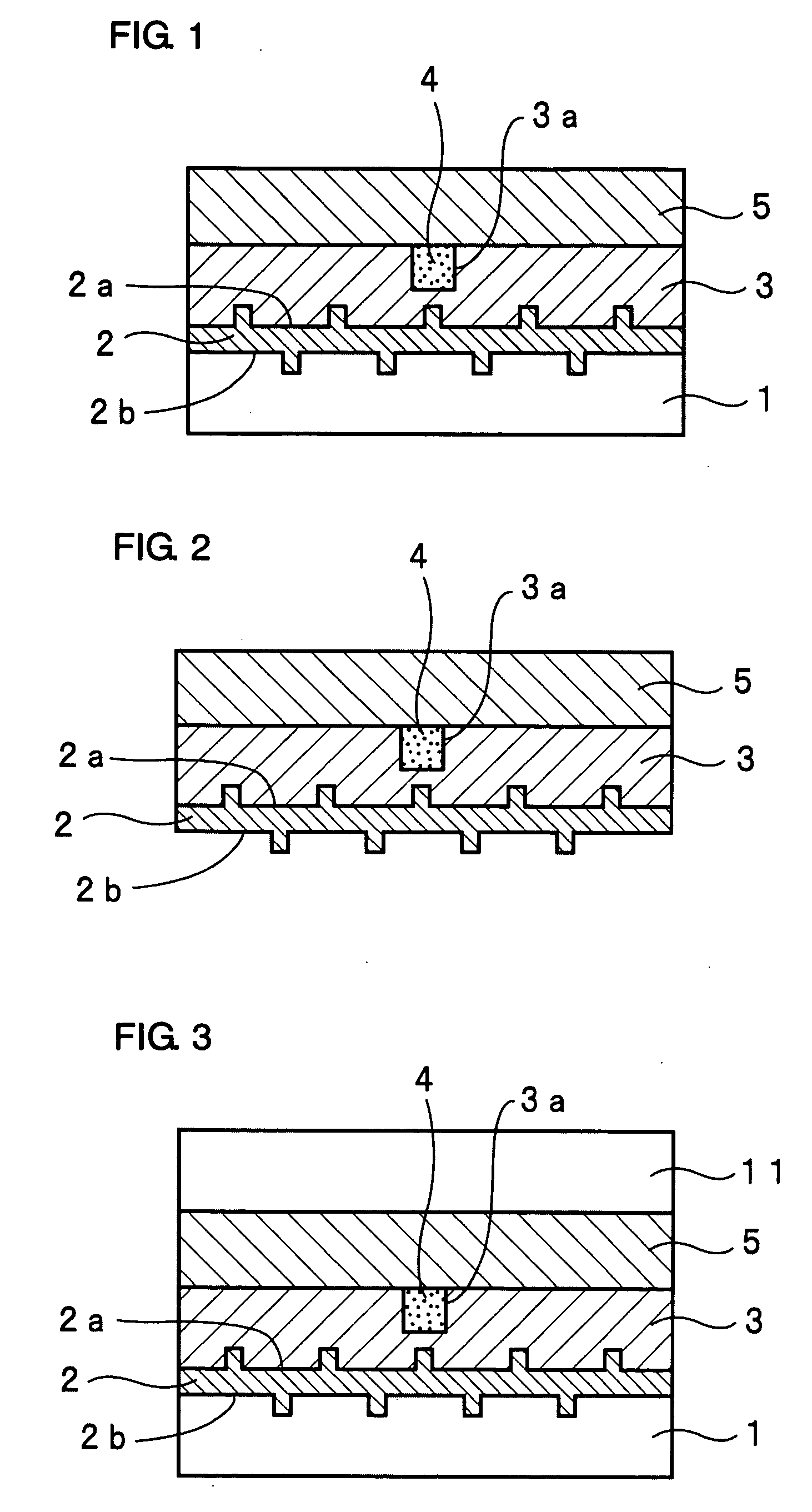
[0126] A four-branch optical waveguide was fabricated for each of the substrates having different thicknesses by following the same procedure as in Example 1 except for using a mold 6 having recesses and projections, the surface roughness Rz of which was 400 nm, as a mold for forming recesses and projections on the surface of the ultraviolet control region 2 in Example 1.

[0127] The fabricated four-branch optical waveguide was observed with an optical microscope, and as a result of this, any of recesses and projections on the surface of the substrate and on an interface of the lower clad layer and the ultraviolet control region has the surface roughness Rz per a length of 250 μm of 400 nm.

[0128] And, the insertion losses of the four-branch optical waveguides were measured in the same way as in Example 1. As a result of this, branch-to-branch variations of the insertion loss were 0.2 dB in any cases of using the substrates having different thicknesses.

[0129] It was found from the a...

example 3

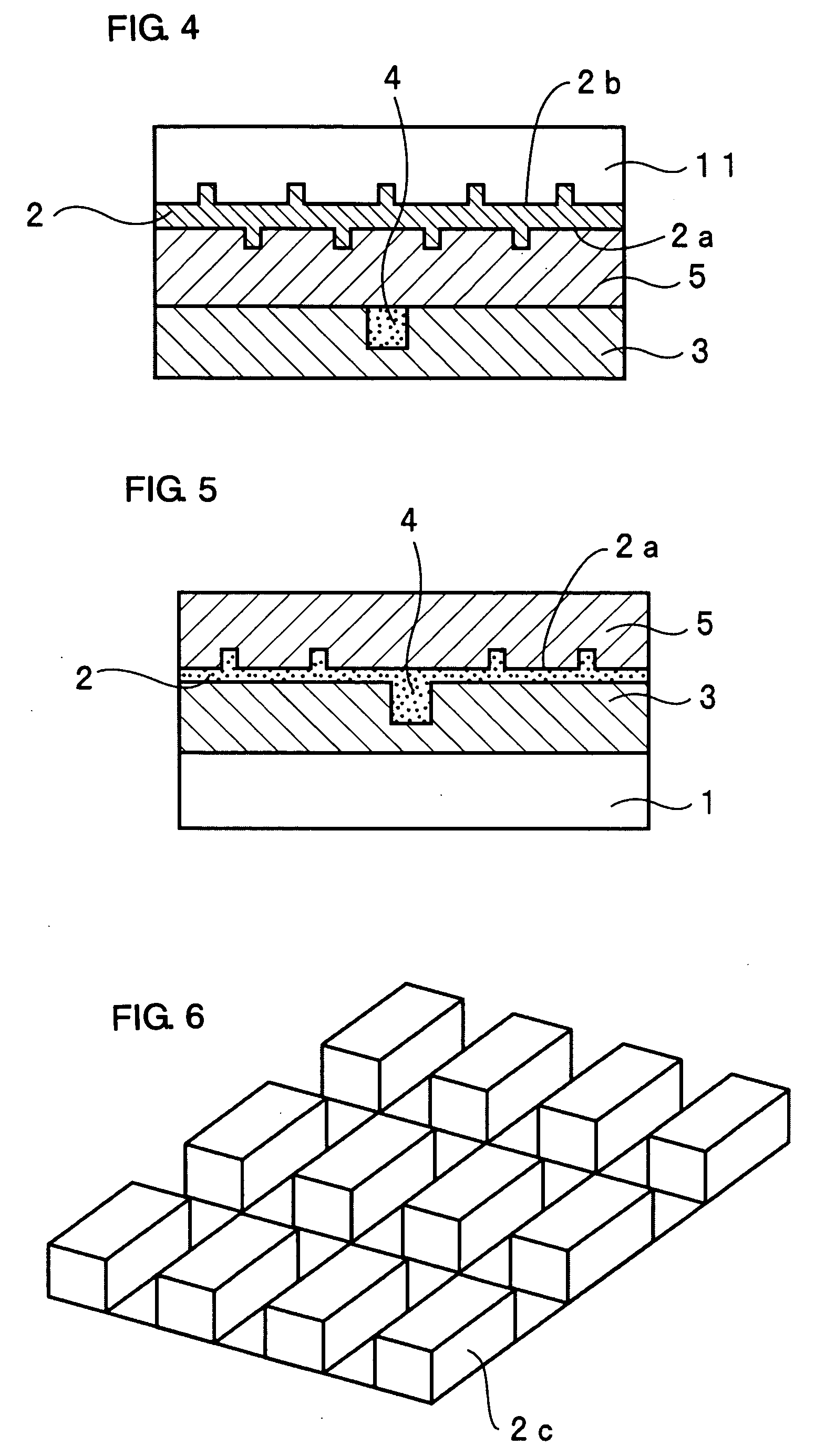
[0130] As a mold 6 for forming recesses and projections on the surface of the ultraviolet control region 2, a mold with the configuration of recesses and projections having the form of stripes, which having a projection portions 2d having the form of stripes as shown in FIG. 7. In addition, the surface roughness Rz of these recesses and projections was 100 nm.

[0131] A four-branch optical waveguide was fabricated for each of the substrates having different thicknesses by following the same procedure as in Example 1 except for using the above-mentioned mold 6. The fabricated four-branch optical waveguide was observed with an optical microscope, and as a result of this, the surface roughness Rz per a length of 250 μm of recesses and projections on an interface of the lower clad layer and the ultraviolet control region was 100 nm.

[0132] And, the insertion losses of the four-branch optical waveguides were measured in the same way as in Example 1. As a result of this, branch-to-branch v...


PUM


Abstract

Disclosed herein is an optical waveguide comprising a core layer to be an optical waveguide region, an upper clad layer covering the core layer and a lower clad layer, characterized in that an ultraviolet control region for preventing ultraviolet light from entering is provided at any one location of under the lower clad layer, on an interface of the lower clad layer and the upper clad layer, and on the upper clad layer. And a method of fabricating this optical waveguide is also disclosed.

Description

[0001] The priority Japanese Patent Application Number 2004-76053 upon which this patent application is based is hereby incorporated by reference. BACKGROUND OF THE INVENTION [0002] 1. Field of the Invention [0003] The present invention relates to an optical waveguide and a method of fabrication thereof. [0004] 2. Description of the Related Art [0005] In recent years, under circumstances where the trend of Internet toward broadband moves forward, it is necessary to reduce a large amount of the cost of devices for optical communication for wide spread use of access such as FTTH. Optical transmitter and receiver modules to convert light to electrical signals are used in terminals of equipment for optical communication as a device for optical communication. In order to bring this optical transmitter and receiver module down in size and cost, there is proposed a method in which an optical waveguide, being a part within the module, is formed from an organic polymeric material (Nobuo Miya...

Claims


Application Information

Patent Timeline
Patent Type & Authority Applications(United States)
IPC IPC(8): G02B6/122G02B6/138G02B6/13H01L21/00
CPCG02B6/138
Inventor NAKAGAWA, YOUHEIHAYASHI, NOBUHIKOKURAMOTO, KEIICHIMATSUMOTO, MITSUAKIHIRANO, HITOSHI
Owner SANYO ELECTRIC CO LTD
Why Eureka
Try Eureka