Optical switch element and its manufacturing method

An optical switch and component technology, which is applied in the manufacture of optical components, optics, semiconductor/solid-state devices, etc., can solve the problems of uneven impurity diffusion refractive index, inability to provide selectivity, uneven film thickness distribution, etc.

Inactive Publication Date: 2005-09-07
FUJITSU SEMICON LTD
View PDF2 Cites 0 Cited by
  • Summary
  • Abstract
  • Description
  • Claims
  • Application Information

AI Technical Summary

Problems solved by technology

[0004] However, when the core material is deposited by means of the above-mentioned flame hydrolysis deposition method, there is a problem that a large difference in impurity diffusion in the core material causes non-uniformity of the refractive index, and non-uniform thickness distribution in the film to be deposited
[0005] Another problem is that when the core is formed by patterning on the lower cladding layer, since the lower cladding layer and the core material formed of almost the same material have a small difference in etching speed, it cannot provide a sufficient selection rate, so during the formation of the core , the lower cladding is also etched so that the desired shape of the core cannot be obtained
In particular, the sidewalls of the core do not form a vertical face, but a rough face with a creeping skirt, which leads to light attenuation

Method used


Image

  • Optical switch element and its manufacturing method
  • Optical switch element and its manufacturing method
  • Optical switch element and its manufacturing method

Examples


Embodiment Construction

[0027] Hereinafter, a preferred embodiment to which the present invention is applied will be described in detail with reference to the accompanying drawings.

(Specific embodiment)

[0028] General structure of optical switching element

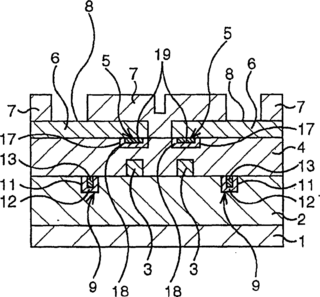
[0029] figure 1 It is a schematic cross-sectional view showing the general structure of the optical switch element according to the present embodiment.

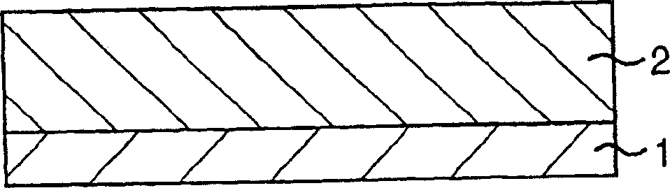
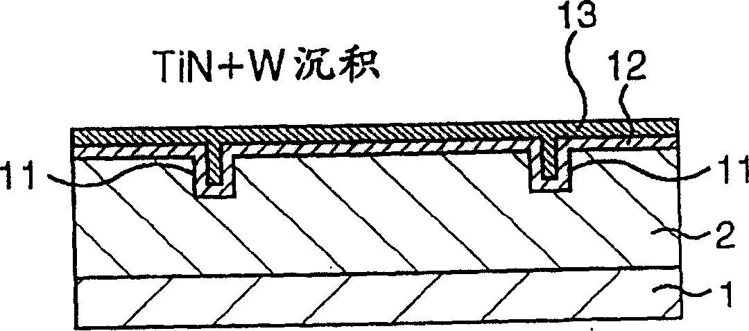
[0030] The optical switch element includes a silicon semiconductor substrate 1; an under-cladding layer 2 formed of a silicon oxide film on the silicon semiconductor substrate 1; each formed of a silicon oxide film and patterned on the under-cladding layer 2 so as to constitute a core 3 of an optical path; and Composed of a silicon oxide film formed on the lower cladding layer 2 so as to cover the upper cladding layer 4 of the core 3; heaters 5 composed of TiN and W sequentially embedded in the grooves formed above the core 3 The position corresponds to the surface layer part of the upper clad...


PUM

PropertyMeasurementUnit
thicknessaaaaaaaaaa
thicknessaaaaaaaaaa
refractive indexaaaaaaaaaa

Abstract

A lower clad, cores, and an upper clad are formed by a chemical vapor deposition method (CVD method). At least one of the additional amount of oxygen, the additional amount of nitrogen, and the additional amount of silicon of a silicon oxynitride film is adjusted so that the cores have a desired higher refractive index than those of the clads. Further, end point detectors are formed which become etching stoppers of dry etching in pattern forming the cores.

Description

[0001] This application is based on prior Japanese Patent Application Nos. 2002-077130 (application date March 19, 2002) and 2003-49867 (application date February 26, 2003), and claims the right of priority. The Japanese patent application is incorporated herein by reference. Technical field [0002] The present invention relates to an optical switching element formed on a semiconductor substrate by using semiconductor process technology and having an optical function corresponding to an optical fiber, and a method for manufacturing the optical switching element. Background technique [0003] Generally, when manufacturing optical switching elements, such as SiCl 4 Such raw material gases flow into the oxy-hydrogen combustion chamber, by means of the flame hydrolysis deposition method, the oxidation reaction is promoted in the flame, thereby depositing the lower cladding layer and the core material in the form of glass particle layer on the silicon substrate. Such as TiO 2 Or GeO 2...

Claims


Application Information

Patent Timeline
Patent Type & Authority Patents(China)
IPC IPC(8): G02B6/13G02B6/12G02F1/01G02F1/313
CPCG02F2202/105G02B2006/12176G02F1/0147G02B2006/12145G02B2006/12197G02B6/12G02F1/3133
Inventor 奥田章二
Owner FUJITSU SEMICON LTD
Why Eureka
Try Eureka