Integrated circuit, semiconductor device and ID chip

a semiconductor and integrated circuit technology, applied in the direction of instruments, liquid/fluent solid measurement, sustainable buildings, etc., can solve the problems of reducing operating margin, large power consumption, and difficult to achieve stable power supply, and achieve high impact resistance and high impact resistance. , the effect of low cos

Inactive Publication Date: 2005-09-22
SEMICON ENERGY LAB CO LTD
View PDF13 Cites 65 Cited by
  • Summary
  • Abstract
  • Description
  • Claims
  • Application Information

AI Technical Summary

Benefits of technology

[0007] In view of the foregoing, the invention provides an integrated circuit, a semiconductor device and an ID chip at low cost where stable operation is achieved by suppressing the power consumption as low as possible and a high impact resistance is assured even when a large circuit area is used.
[0012] The invention provides an integrated circuit and a semiconductor device formed in large quantities over a glass substrate that is larger and cheaper than a silicon wafer so as to improve cost performance. Further, the invention provides a semiconductor device that is formed by peeling elements off a glass substrate and transferring them to a flexible substrate so as to improve an impact resistance. The elements peeled off the glass substrate are 5 μm thick or less (more preferably, 0.1 to 3 μm), therefore, it may be directly stuck to a product container, a tag or the like, or a periphery thereof may be filled with an organic resin material and the like.
[0014] According to the invention, a highly impact-resistant semiconductor device can be provided at low cost. With the high impact resistance ensured, the semiconductor device can have various applications. Furthermore, with the low cost ensured, applications to various products or objects can be expected.
[0015] Furthermore, the invention enables a low power consumption, thereby a semiconductor device having a large operating margin and capable of stable operation can be provided. Accordingly, the reliability of the semiconductor device can be increased, which can improve the reliability of various products or objects to which the semiconductor device of the invention can be applied.

Problems solved by technology

However, according to such a method, the amount of power supplied to the ID chip changes when the positional relationship between the ID chip in operation and the reader / writer changes, and thus a stable power supply is difficult to be achieved.
In addition, since a CPU and a logic circuit for cryptographic operation occupy large circuit areas, a large power consumption is required.
When a stable power supply is unavailable and a large power consumption is required, an operating margin is decreased, which hinders the stable operation.
In addition, the large circuit area will lead to a lower impact resistance of the semiconductor device, and thus the number of chips taken from a silicon wafer is decreased, which leads to a higher cost.

Method used


Image

  • Integrated circuit, semiconductor device and ID chip
  • Integrated circuit, semiconductor device and ID chip
  • Integrated circuit, semiconductor device and ID chip

Examples


embodiment mode 1

[Embodiment Mode 1]

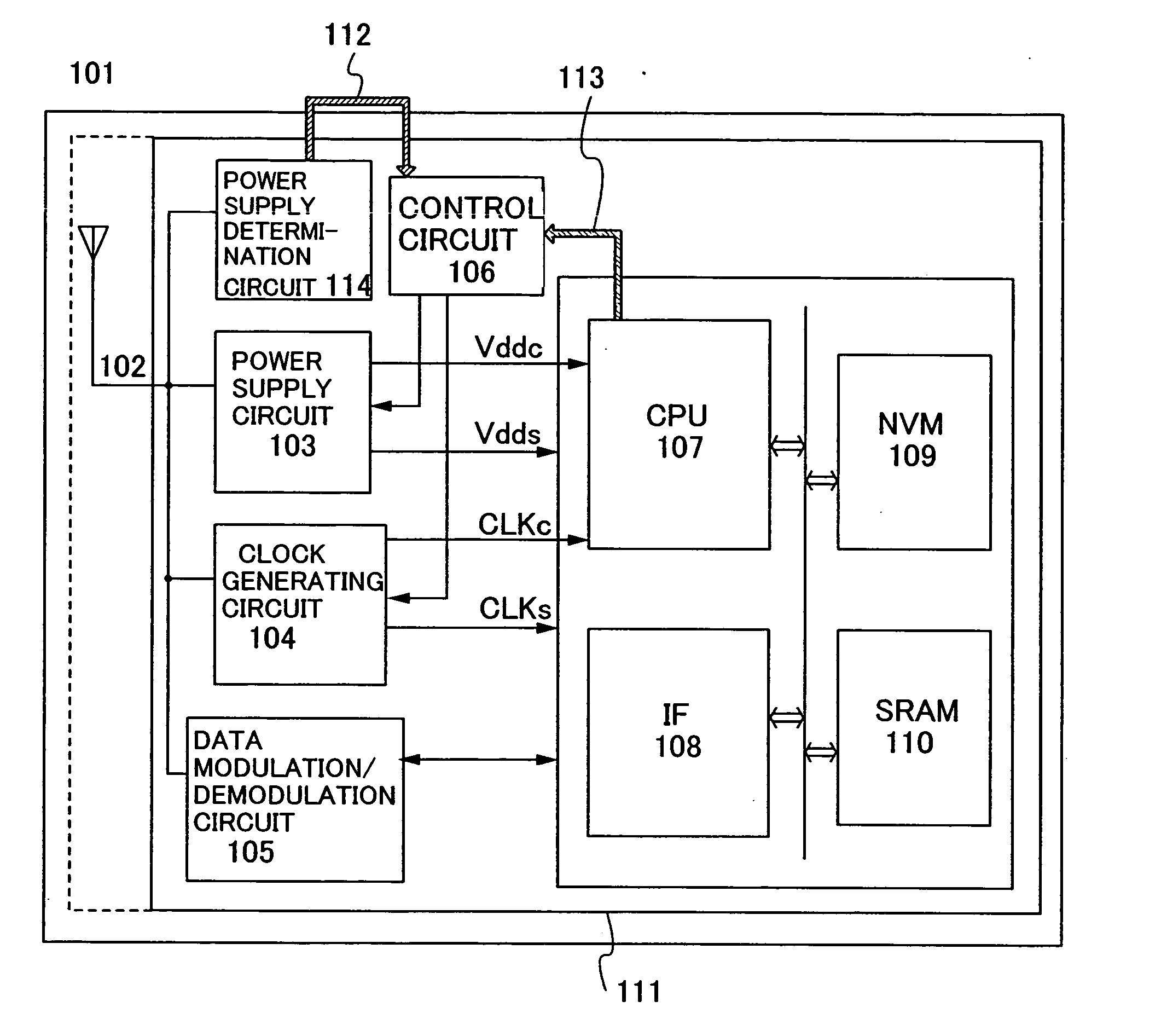
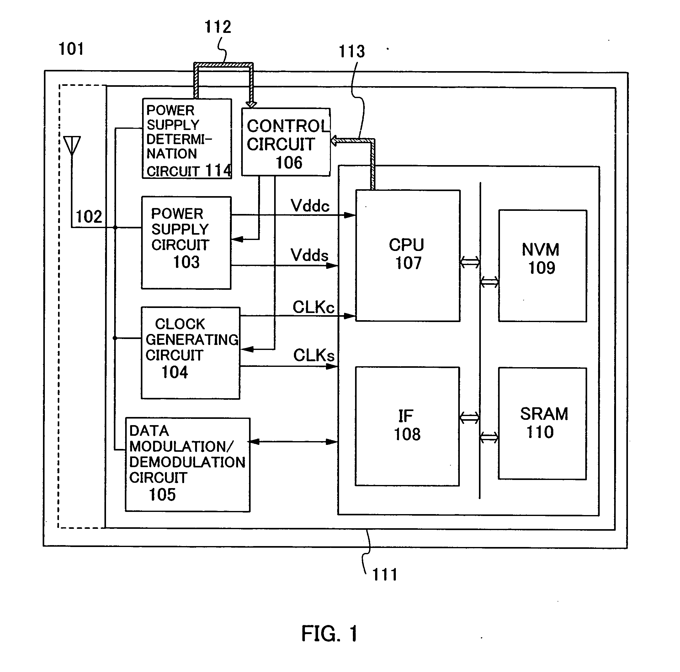
[0030] A configuration of a semiconductor device 101 of the invention is described with reference to FIG. 1. The semiconductor device 101 comprises an integrated circuit 111 and an antenna 102. The integrated circuit 111 comprises a power supply circuit 103, a clock generating circuit 104, a data modulation / demodulation circuit 105 having a data modulating / demodulating function, a control circuit 106, a circuit for determining a power supply level (hereinafter also abbreviated to a power supply determination circuit) 114, a CPU 107, an interface (denoted by an IF in the drawing) 108, a non-volatile memory (denoted by an NVM in the drawing) 109 and an SRAM 110. Note that the SRAM 110 may be substituted with a volatile memory such as a DRAM.

[0031] The integrated circuit 111 is formed over a glass substrate or a flexible substrate. The antenna 102 may be formed either over the same substrate as the integrated circuit 111 in the semiconductor device 101 or over a pro...

embodiment mode 2

[Embodiment Mode 2]

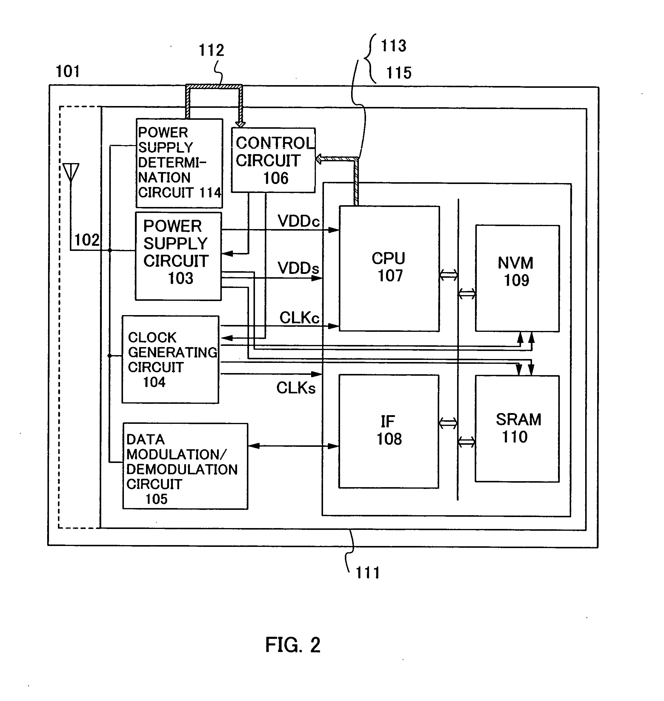
[0043] The configuration of the semiconductor device 101 of the invention is described with reference to FIG. 2. In this embodiment mode, a mode is shown where the control circuit 106 controls memories such as an SRAM and an NVM in addition to the CPU 107.

[0044] The semiconductor device 101 has similar components to the semiconductor device 101 shown in FIG. 1 although it is partially different as for the control signal, the power supply potential and the clock signal. What are different from the semiconductor device 101 shown in FIG. 1 are mainly that the control circuit 106 controls a power supply potential and a clock signal supplied to each memory (the NVM 109 and the SRAM 110), and that the control circuit 106 receives a memory access signal 115 in addition to the power supply data signal 112 and the event signal 113.

[0045] The semiconductor device 101 in this embodiment mode sets an operating mode of a power supply potential and a clock signal correspondin...

embodiment 1

[Embodiment 1]

[0054] In this embodiment, description is made on a power supply circuit for generating a power supply potential, a clock generating circuit and a control circuit each having a different configuration from the aforementioned embodiment modes with reference to FIGS. 3 to 5. Note that common circuits and signals among FIGS. 3 to 5 are denoted by common reference numerals.

[0055] First, description is made on the example where a control circuit is provided in each block of the CPU, the NVM and the SRAM with reference to FIG. 3.

[0056] When a control circuit is provided in each of the CPU 107, the NVM 109 and the SRAM 110, each of the control circuits receives the power supply data signal 112. The control circuit generates an instruction signal for adjusting the power supply potential and the clock frequency in accordance with the power supply level within the range that the total power consumption of each block does not surpass the power supply. The generated instruction ...


PUM

PropertyMeasurementUnit
thickaaaaaaaaaa
thickaaaaaaaaaa
thicknessaaaaaaaaaa

Abstract

A contactless semiconductor device is provided where a low power consumption is achieved and wireless communication is carried out stably. A power supply level of a reader / writer and the operating state of internal blocks of an ID chip are monitored. In accordance with such conditions, a clock signal of an optimal frequency and a power supply potential of an optimal level are selected to be supplied. By setting the operating mode in accordance with the power supply level or the power saving mode in accordance with the operating state of each block, a low power consumption ID chip and stable wireless communication can be provided.

Description

BACKGROUND OF THE INVENTION [0001] 1. Field of the Invention [0002] The present invention relates to an integrated circuit, a semiconductor device and an ID chip formed over a glass substrate or a flexible substrate. In addition, the invention relates to an integrated circuit, a semiconductor device and an ID chip that establish contactless communication. [0003] 2. Description of the Related Art [0004] In recent years, a contactless IC card, ID tag, RFID or the like (hereinafter collectively referred to as an ID chip) having a high security function has been increasingly demanded for the purpose of ID management of securities, cashless electronic payment and the like by use of the ID chip. Such an ID chip incorporates highly functional integrated circuits such as a central processing circuit (typically referred to as a central processing unit and hereinafter also abbreviated to CPU) and a dedicated hardware having a cryptographic function. [0005] An ID chip receives a power supply t...

Claims


Application Information

Patent Timeline
Patent Type & Authority Applications(United States)
IPC IPC(8): G06F1/26G06F1/32G06K7/00G06K19/07G07F7/08G07F7/10H01L21/82H01L27/02
CPCG06K7/0008G06K19/0701G06Q20/32G06Q20/327Y02B60/50G06Q20/40145G07F7/0866G07F7/1008G06Q20/341A41C3/12A41C5/005A41C3/10
Inventor KATO, KIYOSHIKOYAMA, JUN
Owner SEMICON ENERGY LAB CO LTD
Why Eureka
Try Eureka