IC package, inspection method of IC package mounting body, repairing method of IC package mounting body, and inspection pin for IC package mounting body

Inactive Publication Date: 2005-09-29
KK TOSHIBA
View PDF5 Cites 6 Cited by
  • Summary
  • Abstract
  • Description
  • Claims
  • Application Information

AI Technical Summary

Benefits of technology

[0015] According to the present invention, a faulty connection is easily detected and the defect can be reduced in an IC package being an outer package to package a semiconductor chip and others on an substrate and so on, an inspect

Problems solved by technology

In such a packaging process, there are some typical defective modes in its electrical and mechanical connection, such as what is called a solder bridge which is a short-circuit between solder balls by soldering, and what is called an unsoldering defect in which the solder balls are not connected to the subs

Method used


Image

  • IC package, inspection method of IC package mounting body, repairing method of IC package mounting body, and inspection pin for IC package mounting body
  • IC package, inspection method of IC package mounting body, repairing method of IC package mounting body, and inspection pin for IC package mounting body
  • IC package, inspection method of IC package mounting body, repairing method of IC package mounting body, and inspection pin for IC package mounting body

Examples


Example

[0022] Embodiments of the present invention will be described with reference to the drawings, but these drawings are presented only for the illustrative purpose and in no respect, are intended to limit the present invention.

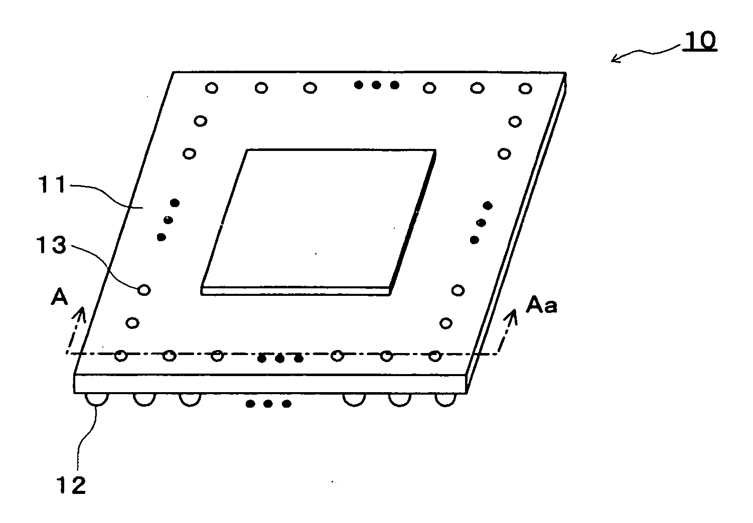
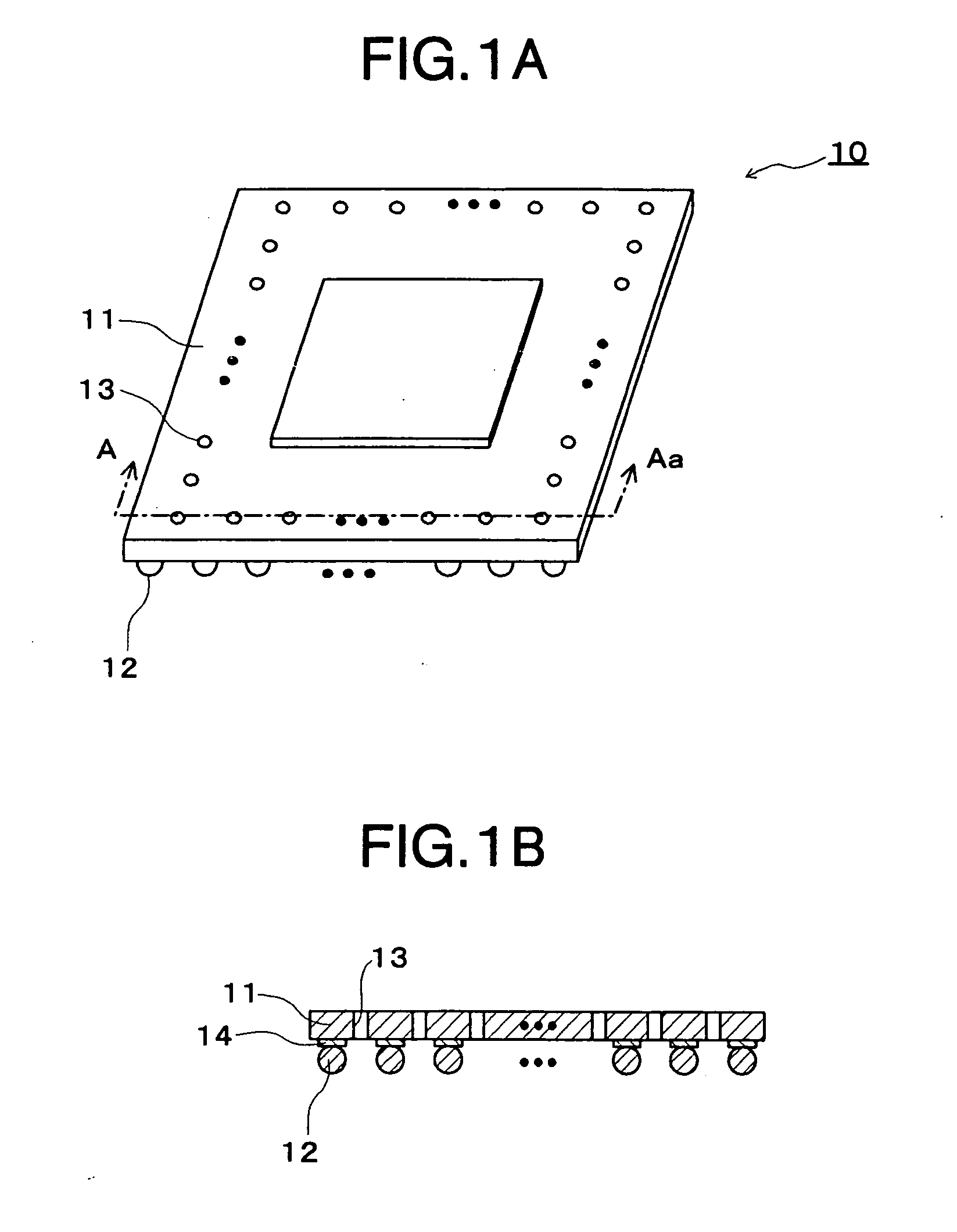
[0023] As a mode of the present invention, the position of penetration hole is on a longitudinal line or a latitudinal line of a grid formed of lands for external connection. It is to respond to a solder bridge which is easy to be formed on the longitudinal line or the latitudinal line of the grid where the distance between adjacent solder balls is short.

[0024] Here, the penetration hole may be provided between the lands for external connection at least in the respective vicinity of the four corners of an interpose substrate. In the vicinity of the four corners of the interpose substrate are the portions where the frequency of the defect occurrence such as a solder bridge is the highest compared to other portions due to various factors. Consequently, it is disp...


PUM


Abstract

Disclosed is an IC package including an interpose substrate and lands for external connection disposed on a face of the interpose substrate in a grid pattern, the interpose substrate having a penetration hole on at least a position between the lands for external connection disposed in a grid pattern. Besides, there are disclosed an inspection method of an IC package mounting body mounting this IC package, a repairing method of an IC package mounting body mounting this IC package, and an inspection pin for an IC package mounting body used for such an inspection.

Description

CROSS-REFERENCE TO THE INVENTION [0001] This application is based upon and claims the benefit of priority from the prior Japanese Patent Application No. 2004-86685, filed on Mar. 24, 2004; the entire contents of which are incorporated herein by reference. BACKGROUND [0002] 1. Field of the Invention [0003] The present invention relates to an IC package being an outer package to package a semiconductor chip and others on a substrate and so on, an inspection method of an IC package mounting body mounting such an IC package, a repairing method of an IC package mounting body mounting such an IC package, and an inspection pin for an IC package mounting body used for such an inspection. Especially, it relates to an IC package, an inspection method of an IC package mounting body, a repairing method of an IC package mounting body, and an inspection pin for an IC package mounting body suitable for reducing the mounting failure. [0004] 2. Description of the Related Art [0005] In an IC package,...

Claims


Application Information

Patent Timeline
IPC IPC(8): H01L23/12H01L21/48H01L21/66H01L23/13H01L23/48H01L23/498H05K3/22H05K3/34
CPCH01L21/485H01L21/4864H01L23/498H05K3/225H05K3/3436H05K3/3494H01L2924/0002H05K2201/09063H05K2203/0126H05K2203/081H01L2924/00Y02P70/50
Inventor OGAWA, HIDEKITANAKA, HIDENORI
Owner KK TOSHIBA
Why Eureka
Try Eureka