High Electron Mobility Transistors and Integrated Circuits with Improved Feature Uniformity and Reduced defects for Microwave and Millimetre Wave Applications

US20150372096A1Inactive Publication Date: 2015-12-24SHIH ISHIANG +3

Image

  • High Electron Mobility Transistors and Integrated Circuits with Improved Feature Uniformity and Reduced defects for Microwave and Millimetre Wave Applications
  • High Electron Mobility Transistors and Integrated Circuits with Improved Feature Uniformity and Reduced defects for Microwave and Millimetre Wave Applications
  • High Electron Mobility Transistors and Integrated Circuits with Improved Feature Uniformity and Reduced defects for Microwave and Millimetre Wave Applications

Examples


Embodiment Construction

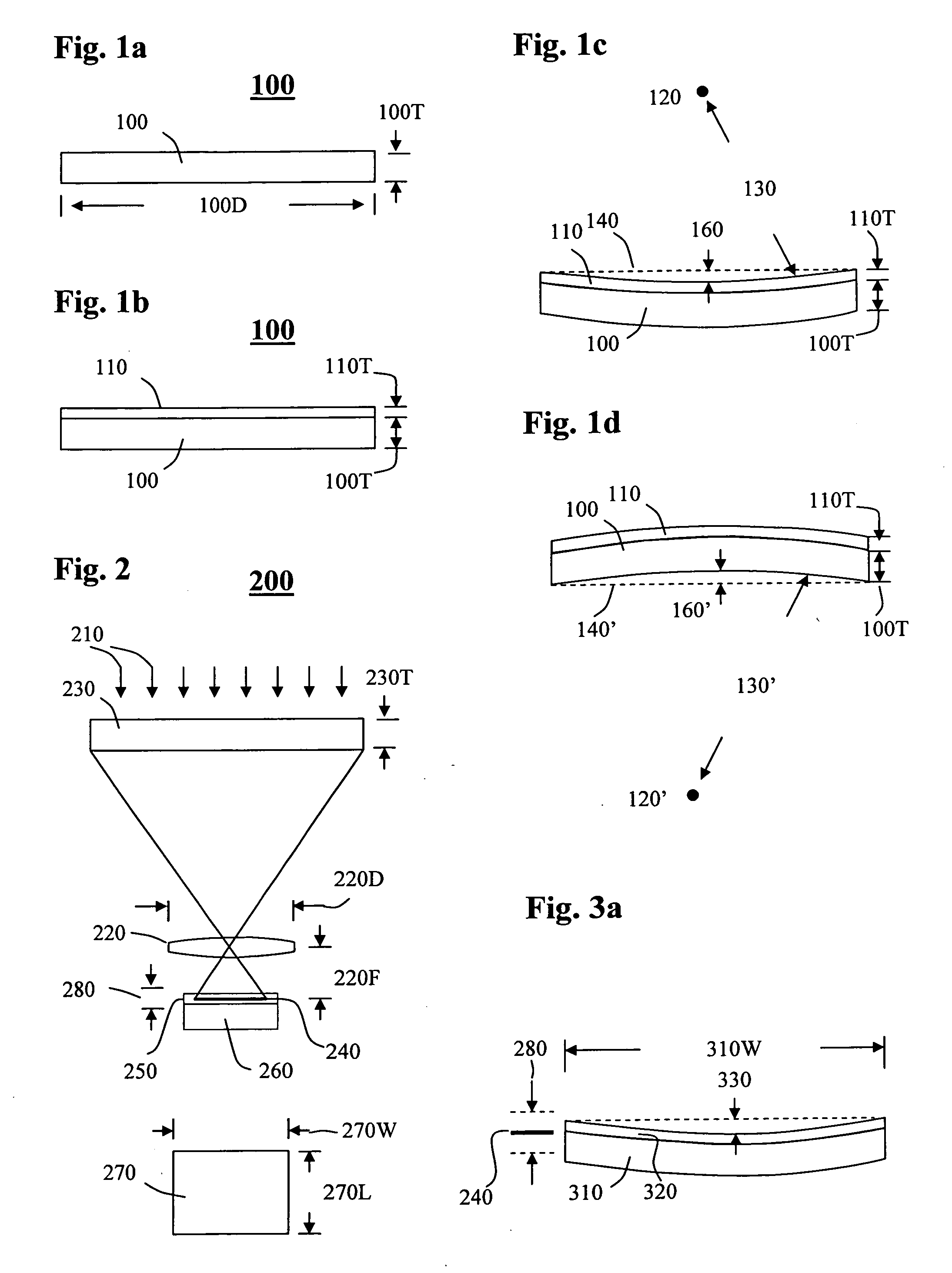
[0019]FIG. 3a shows a portion of a wafer or a substrate (310), with a photoresist layer (320) applied on it and the width of the substrate portion (310W) is substantially the same as the field image width (270W) shown in FIG. 2. The substrate portion (310) has a concave deformation and a bow (330) which is substantially smaller than the depth of focus (DOF, 280) of the stepper or scanner. Under these conditions, when an areal image is projected onto the photoresist layer in the central region, the photoresist layer in the entire field will be within the depth of focus so that uniform critical dimension (CD) (or uniform width of the smallest feature) can be obtained in the entire field.

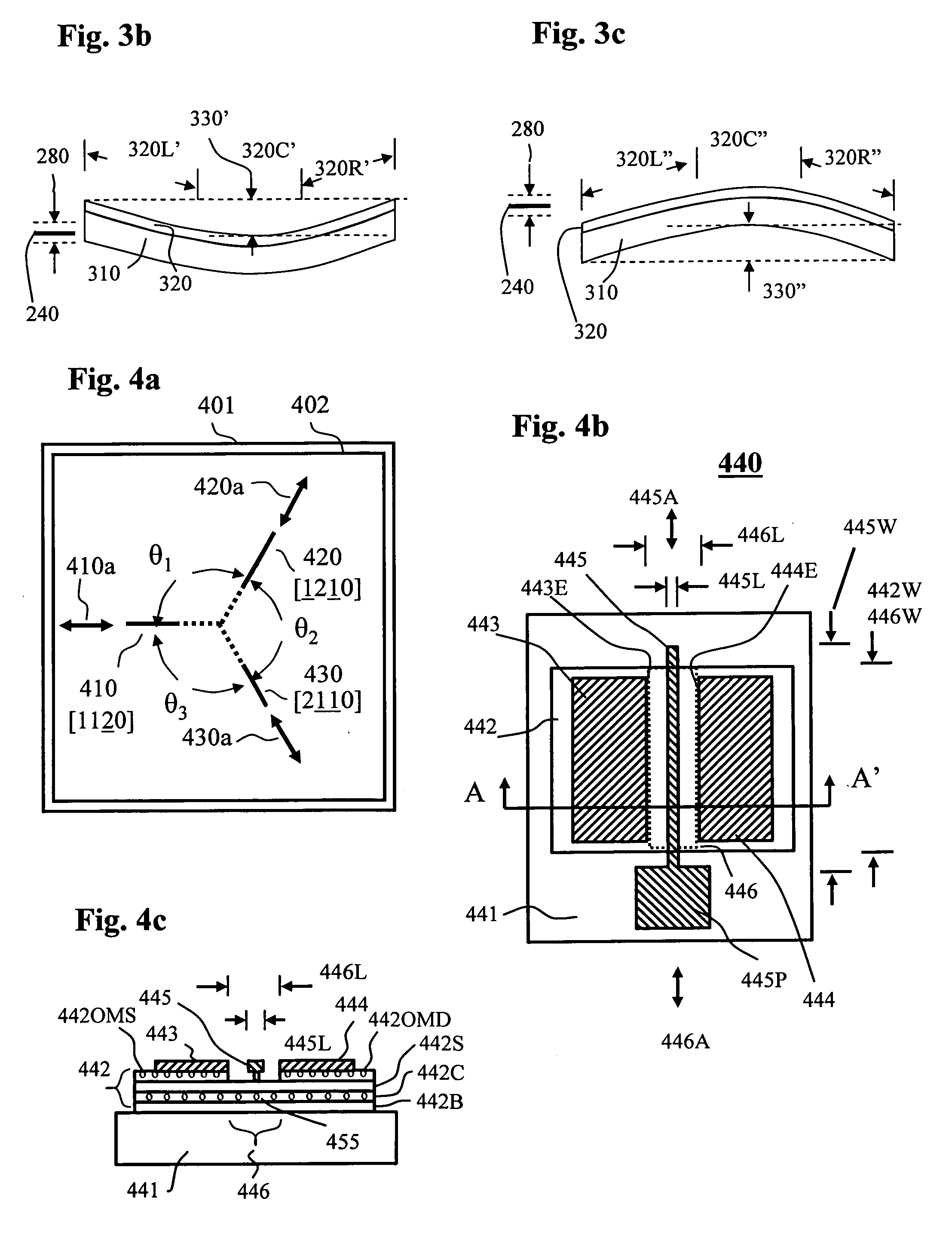
[0020]When the deformation of a concave substrate portion (310) is severe, the bow (330′) is substantially greater than DOF (280) of the imaging system, as shown in FIG. 3b. Under these conditions, when an areal image is projected onto the photoresist surface, only the photoresist layer in the central ...


PUM


Abstract

High mobility transistors and microwave integrated circuits with an improved uniformity of the width of the smallest of features, an increased lithographic yield and reduced defects in the active components are provided. Before and during fabrication, a first grooving process is performed to partially or completely remove composite epitaxial layers in the field lanes to reduce the initial bow to be smaller than DOF range and to improve the uniformity of the critical dimension. A second grooving process may also be performed to remove composite epitaxial layers in the dicing lanes to further improve the uniformity of the width of the smallest features for the devices and circuits to be made.

Description

FIELD OF INVENTION[0001]The present invention is related to transistor devices and circuits for power switching and microwave amplification. More specifically, it is related to high mobility transistors and microwave integrated circuits with improved critical dimension uniformity, increased lithographic yield and reduced defects in the active components.BACKGROUND OF THE INVENTION[0002]In addition to devices based on a metal-oxide-semiconductor (MOS) structure, an insulated gate bipolar transistor (IGBT) structure and a lightly doped drain metal-oxide-semiconductor (LDMOS) structure which are commonly used for power switching and signal amplification, a new class of semiconductors based on III-nitrides are being developed. This is due to the needs to enhance the circuit performance by having higher power handling capability and to reduce the unwanted power loss, beyond what the present silicon-based devices can provide. There is also a need to provide devices which can perform at hi...

Claims


Application Information

Patent Timeline
24 Dec 2015
Publication
US20150372096A1
IPC
H01L29/20; H01L29/778; H01L29/205; H01L27/06
CPC
H01L29/2003; H01L27/0203; H01L21/0274; H01L21/3083; H01L21/3065; H01L21/02664; H01L29/66462; H01L2924/13064
Inventors
SHIH, ISHIANG; QIU, CHUNONG