

Image sensor and method for manufacturing the same
- Summary
- Abstract
- Description
- Claims
- Application Information
AI Technical Summary
Benefits of technology
Problems solved by technology
Method used
Image

Examples
experimental example
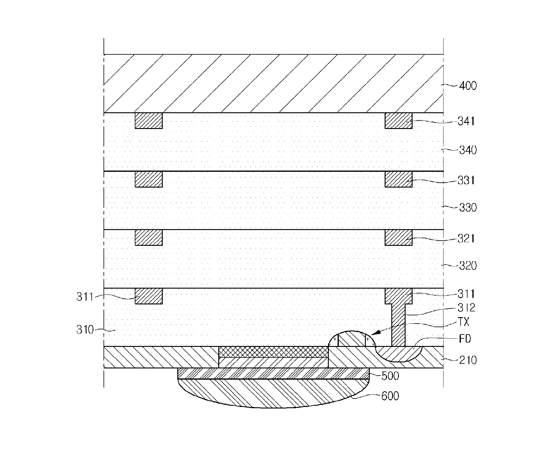
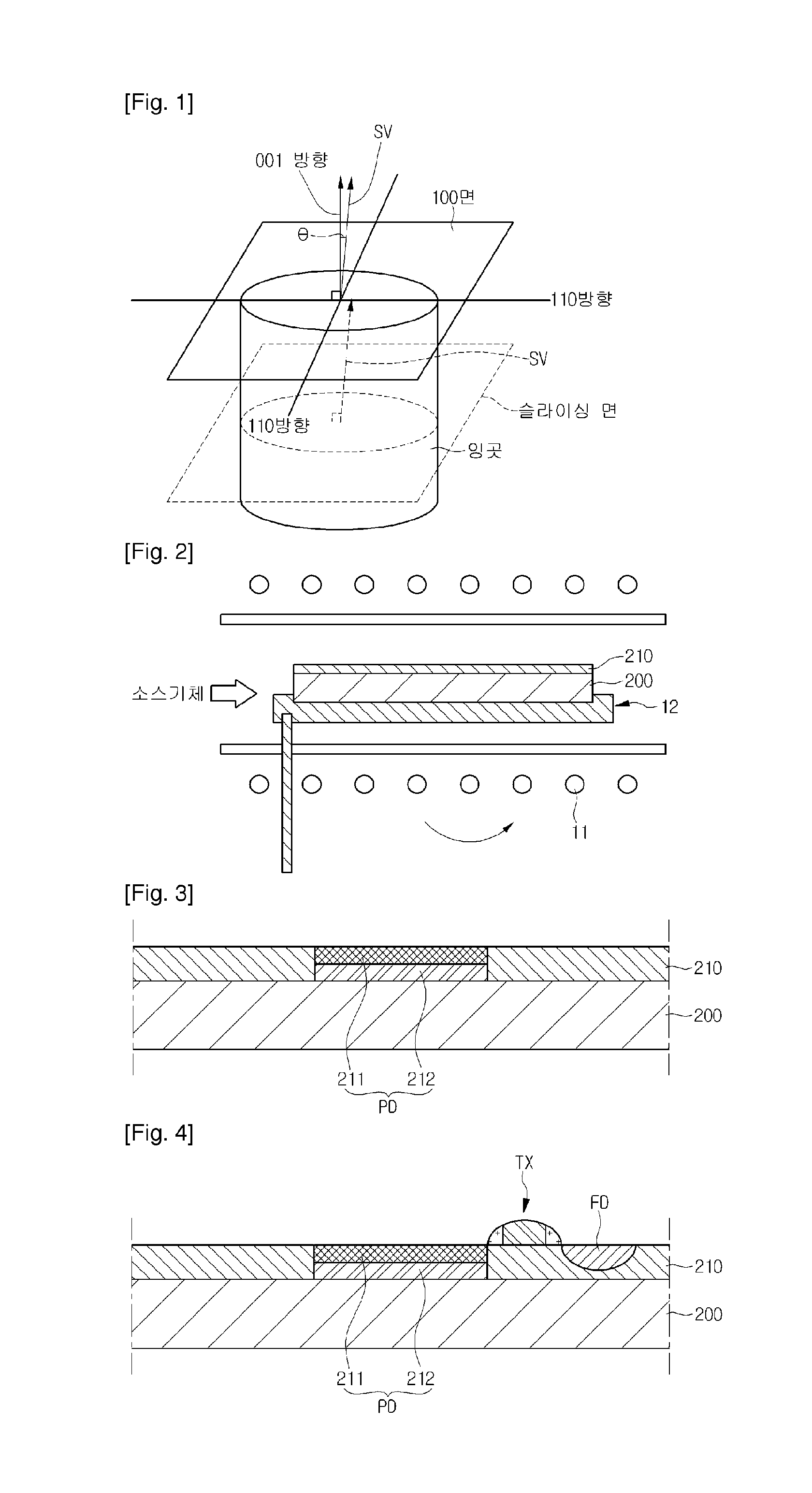
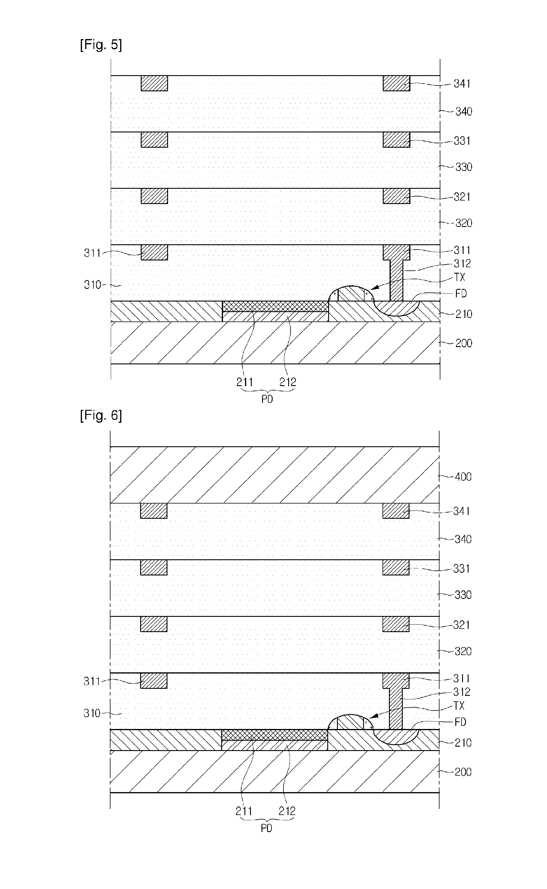
[0061]A silicon ingot having various off angles and a diameter of about 300 mm is grown, and then a slicing and polishing process are performed to form a silicon wafer. Thereafter, an epitaxial layer having a thickness of about 1 μm to about 20 μm is formed using silicon tetrachloride as a source gas and using B2H6 as dopant gas. Thereafter, n-type impurities are injected into the epitaxial layer to form a photodiode. Thereafter, a dual damascene process is performed on the epitaxial layer to form four wire layers. Thereafter, a wafer that is a support substrate is attached to the uppermost wire layer, and the silicon wafer is removed. Then, a color filter and a micro lens are formed under the epitaxial layer.
Result
[0062]As described above, the defects and defect rates of the epitaxial layer formed according the off angle and the image sensor are illustrated in FIGS. 9 and 10. FIG. 9 is a view illustrating the number of defects according to an off angle of an epitaxial layer. FIG. 1...
PUM
 Abstract
Description
Claims
Application Information