Two step trench definition procedure for formation of a dual damascene opening in a stack of insulator layers

a technology of damascene and trench definition, which is applied in the direction of semiconductor/solid-state device manufacturing, basic electric elements, electric devices, etc., can solve the problems of loss of insulator thickness and higher than desired interface resistance, and achieve the effect of reducing the risk of corner rounding and reducing the risk of damag

Inactive Publication Date: 2005-09-29
TAIWAN SEMICON MFG CO LTD
View PDF7 Cites 13 Cited by
  • Summary
  • Abstract
  • Description
  • Claims
  • Application Information

AI Technical Summary

Benefits of technology

[0007] It is another object of this invention to employ a two step, dry etching procedure in the dual damascene opening procedure for removal of the stop or liner layers used as components in the stack of insulator layers, to reduce the risk of corner rounding of a capping insulator layer component of the stack of insulator layers.
[0008] It is still another object of this invention to employ the two step, dry etching procedure in the dual damascene procedure for removal of the stop or liner layers used as components of the stack of insulator layers, to reduce the risk of damage to the top surface of an underlying conductive structure, exposed at the dual damascene opening at the conclusion of the dual damascene opening procedure.

Problems solved by technology

The above procedure can however result in damage to the top surface of the exposed underlying conductive interconnect structure during the trench definition procedure, resulting in possible higher than desired interface resistance when overlaid with an conductive via structure.
In addition other dual damascene opening procedures can also result in loss of insulator thickness as well as corner rounding of the exposed top insulator component of the via opening occurring during various stages of the definition procedure.

Method used


Image

  • Two step trench definition procedure for formation of a dual damascene opening in a stack of insulator layers
  • Two step trench definition procedure for formation of a dual damascene opening in a stack of insulator layers
  • Two step trench definition procedure for formation of a dual damascene opening in a stack of insulator layers

Examples


Embodiment Construction

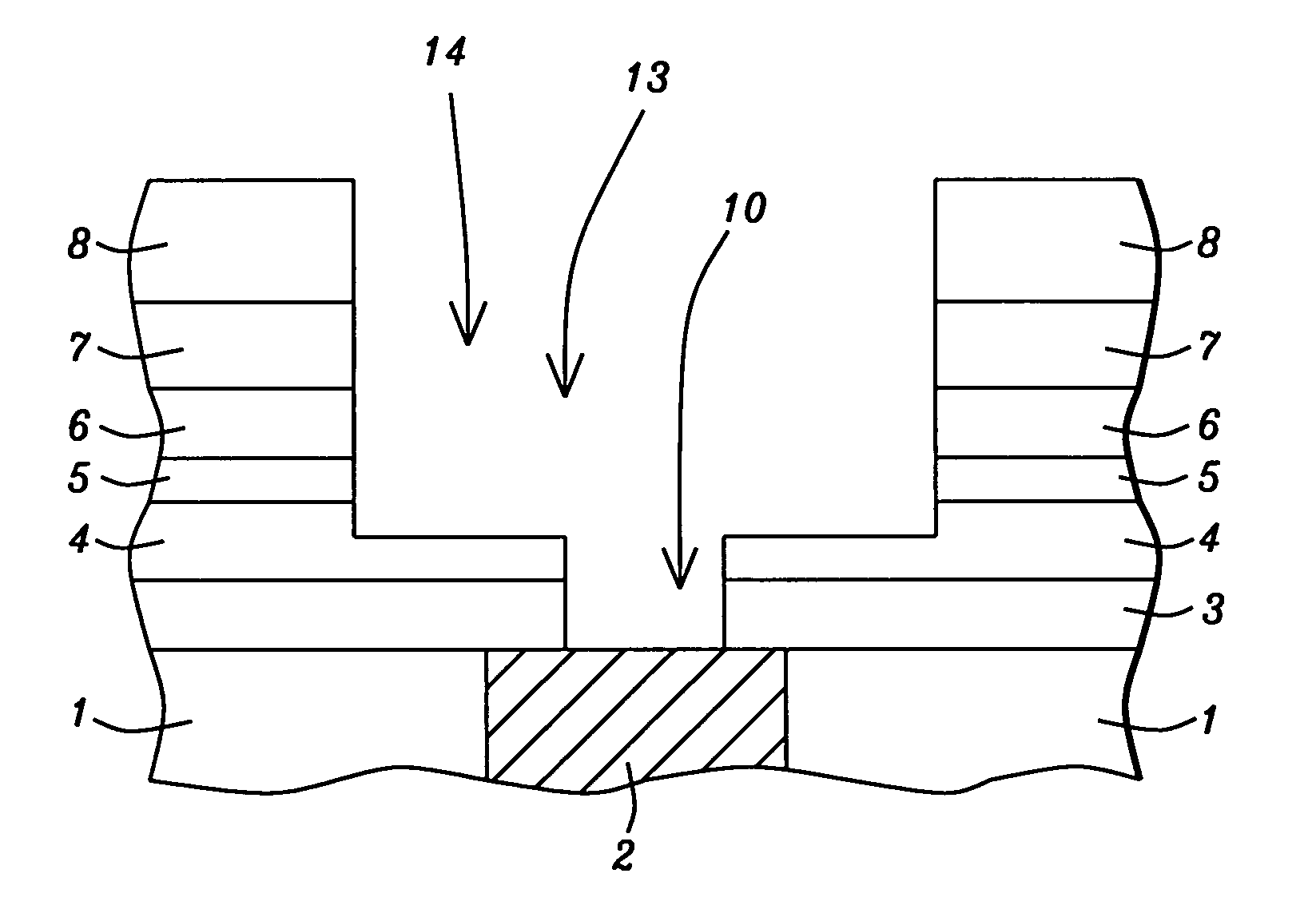
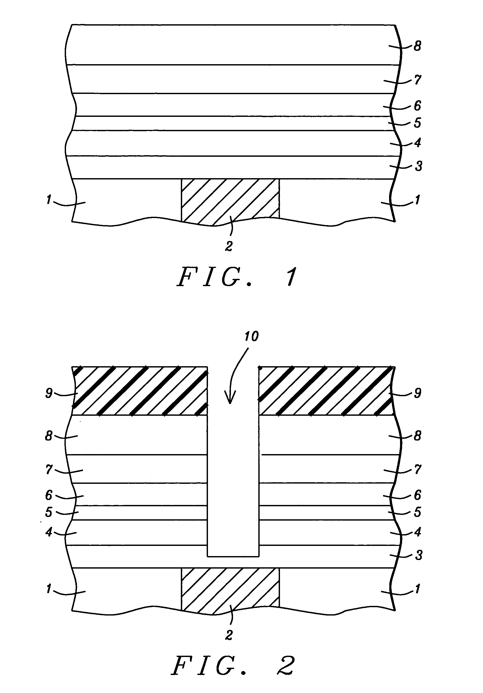
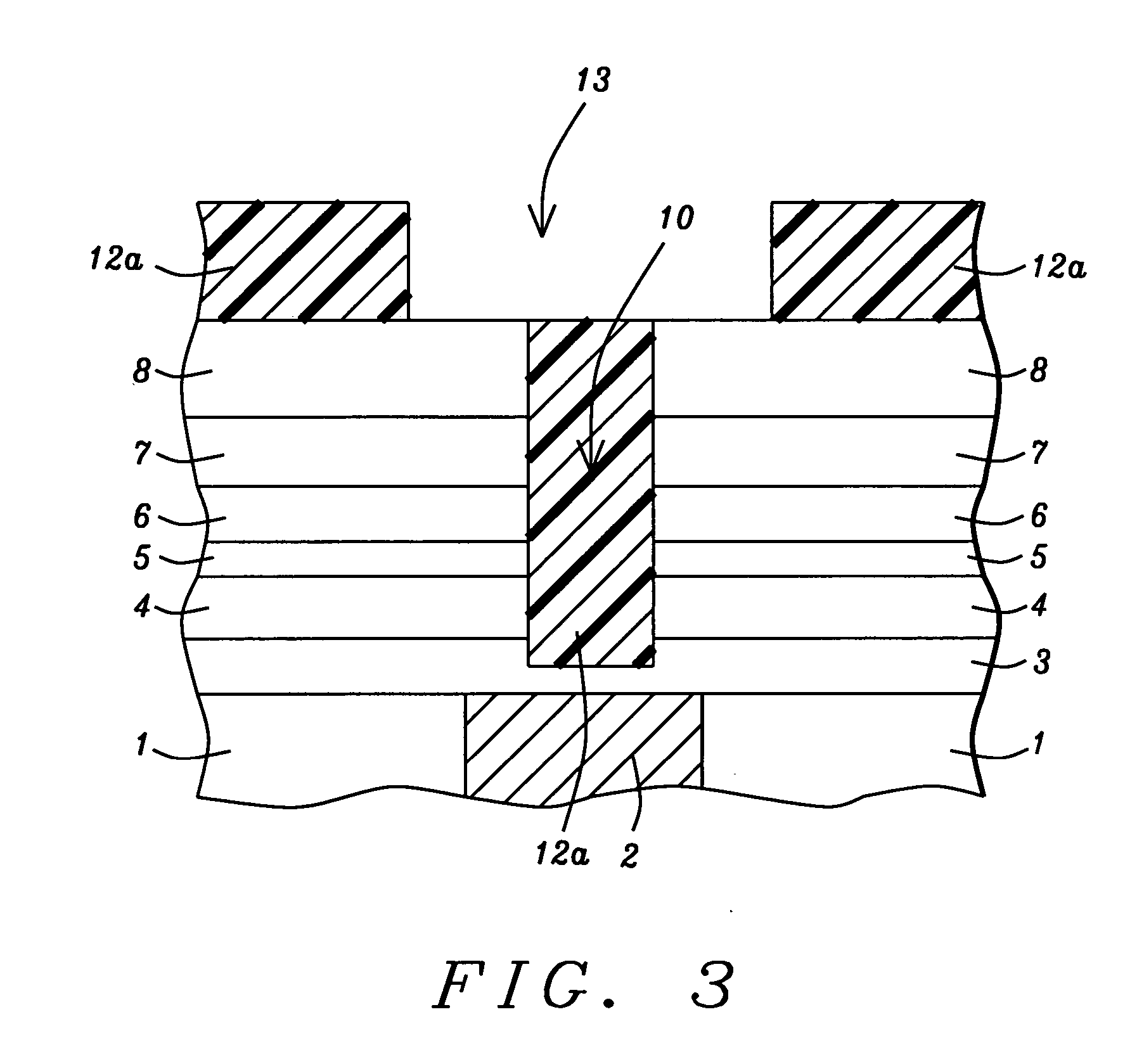
[0012] The method of defining a dual damascene opening in a stack of insulator layers, featuring a two step procedure employed for removal of the stop or liner layer components of the insulator stack, will now be described in detail. Conductive structure 2, a structure comprised of a material such as a copper, is shown schematically shown in FIG. 1, embedded in insulator layer 1, wherein insulator layer 1, can be comprised of silicon oxide, or a boro-phosphosilicate glass (BPSG). First liner or stop layer 3, a layer such as silicon nitride, is deposited to a thickness between about 400 to 600 Angstroms via plasma enhanced chemical vapor deposition (PECVD) procedures. Insulator layer 4, a fluorinated silica glass (FSG) layer, is next formed on first liner layer 3, at a thickness between about 250 to 1000 Angstroms via PECVD procedures. Second liner layer 5, again a layer such as silicon nitride, is next deposited to a thickness between about 200 to 400 Angstroms via PECVD procedures....


PUM


Abstract

A process for defining a dual damascene opening in a stack of insulator layers to expose a portion of a top surface of an underlying conductive structure, has been developed. The process features a two step procedure for removal of insulator stop layers, wherein the stop layers are employed to allow selective dry etch procedures to be used for definition of both the via opening component and the trench shape component of the dual damascene opening. After definition of the via opening, terminating at the top surface of an underlying, first silicon nitride stop layer, a photoresist shape is used as an etch mask to allow a dry etch procedure to define a trench shape in a top portion of an insulator stack, with the dry etch procedure terminating at the top surface of an overlying second silicon nitride stop layer. The dry etch procedure also results in formation of a photoresist plug in the via hole, located on an underlying, first silicon nitride stop layer. The portion of the second silicon nitride stop layer exposed in the trench shape opening is next selectively removed via a first procedure of the two step, dry etch removal procedure, followed by removal of the trench shape defining photoresist shape and of the photoresist plug. Another dry etch procedure, the second step of the two step dry etch removal procedure, is next performed to selectively remove the portion of underlying, first silicon nitride stop layer exposed in the via opening, resulting in exposure of a portion of the top surface of the conductive structure. The two step, stop layer removal procedure reduces the level of insulator corner rounding at the top of the dual damascene opening, while also reducing damage to the top surface of the underlying conductive structure, exposed at the bottom of the dual damascene opening.

Description

BACKGROUND OF THE INVENTION [0001] (1) Field of the Invention [0002] The present invention relates to methods used to fabricate semiconductor devices, and more specifically to a method used to form a dual damascene opening in a stack of insulator layers to expose an underlying conductive gate structure. [0003] (2) Description of the Prior Art [0004] Dual damascene openings formed in insulator layers has enabled conductive via structures as well as overlying conductive interconnect structures to be defined simultaneously in the dual damascene opening. One method of forming a dual damascene opening is to first define a narrow diameter via opening in an entire stack of insulator layers, exposing a top surface of an underlying conductive interconnect structure, followed by definition of a wider diameter trench shape in a top portion of the same insulator layer stack. The above procedure can however result in damage to the top surface of the exposed underlying conductive interconnect str...

Claims


Application Information

Patent Timeline
Patent Type & Authority Applications(United States)
IPC IPC(8): H01L21/4763H01L21/768
CPCH01L21/76813H01L21/76808
Inventor YANG, FU-KAISUEN, SHU-HUEI
Owner TAIWAN SEMICON MFG CO LTD
Why Eureka
Try Eureka