Porous body and manufacturing method therefor
- Summary
- Abstract
- Description
- Claims
- Application Information
AI Technical Summary
Benefits of technology
Problems solved by technology
Method used
Image

Examples
embodiment 1
(1) Embodiment 1
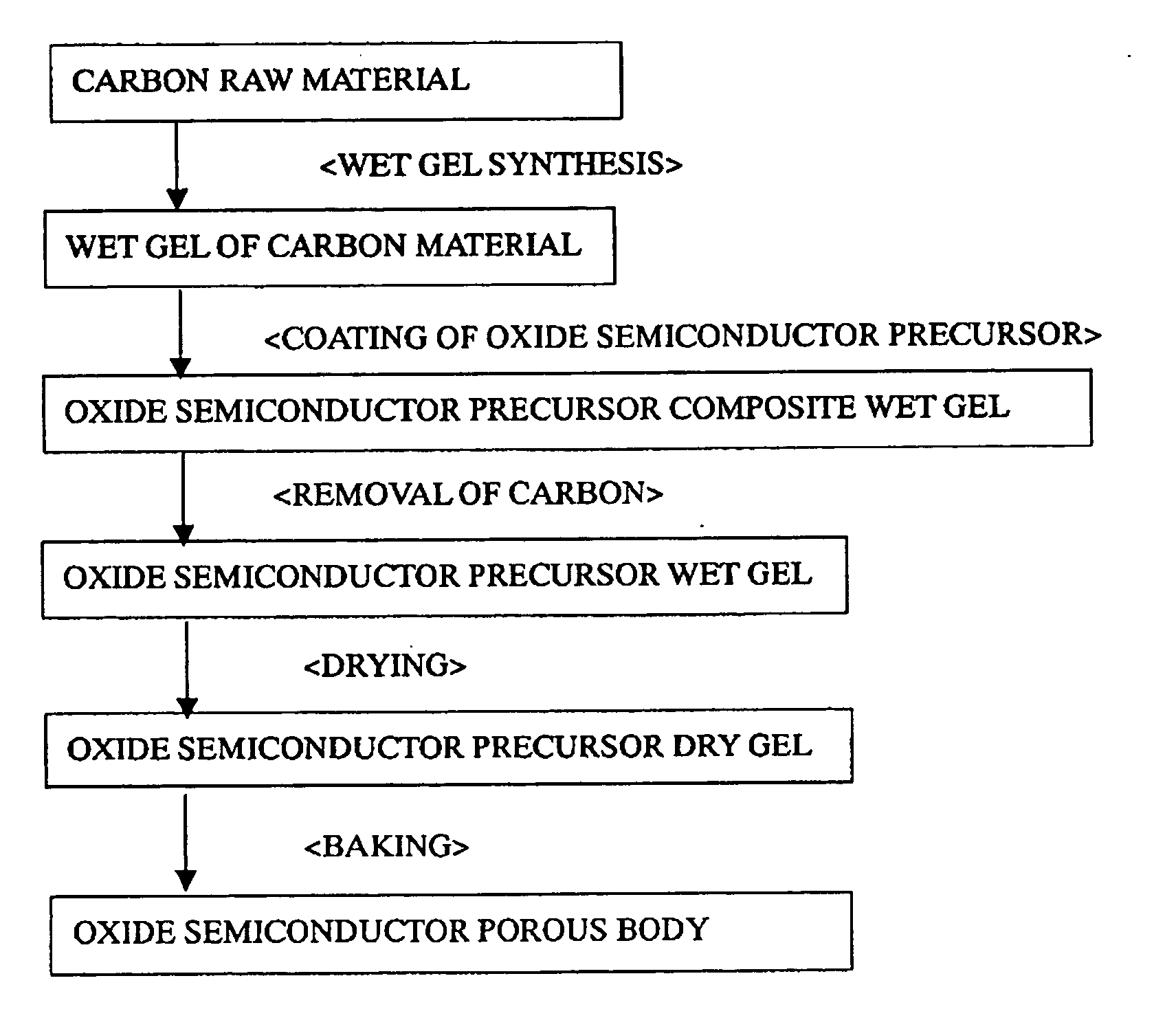
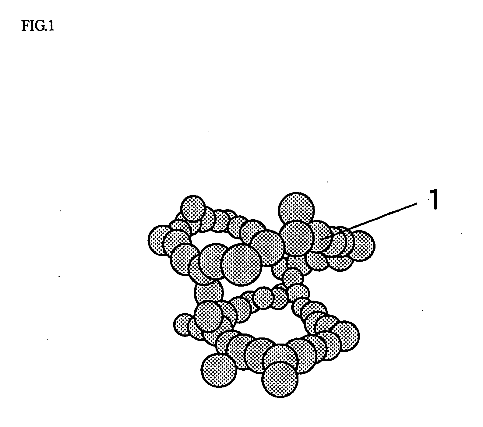
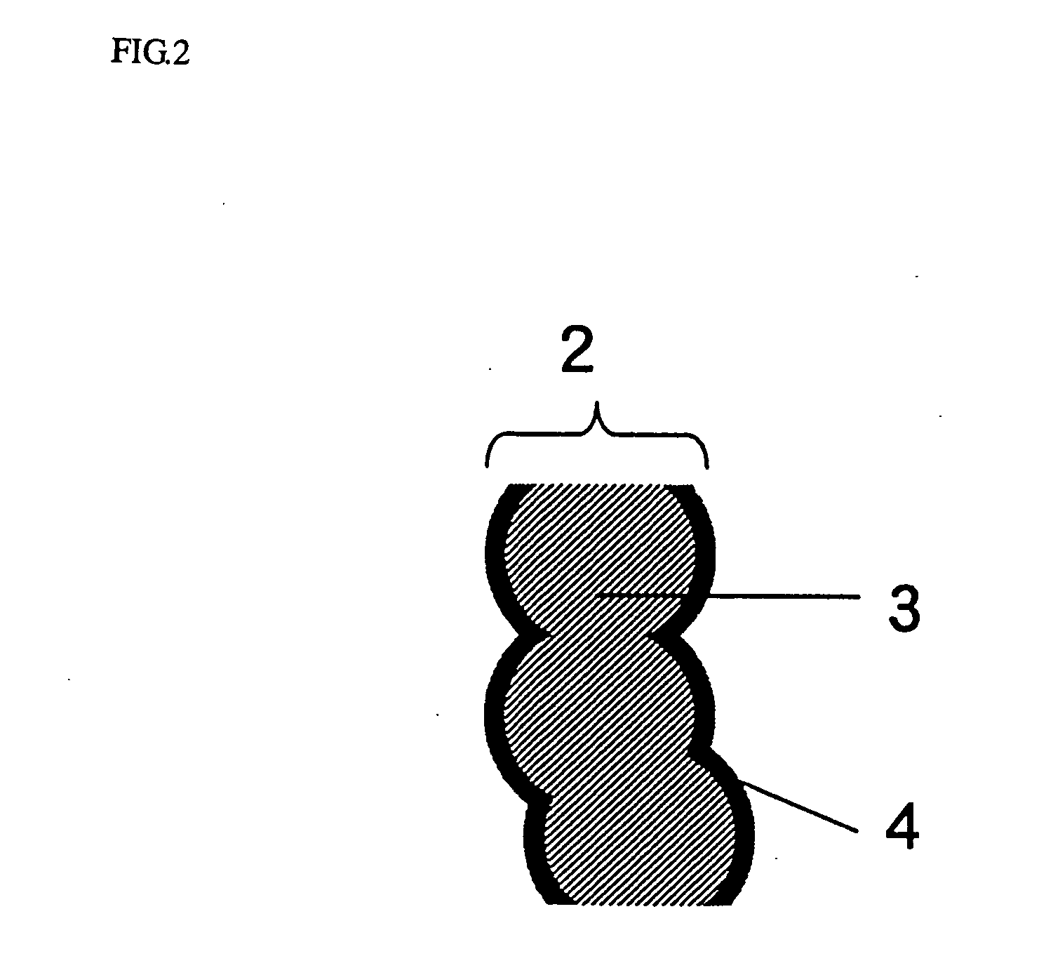
[0111] The first configuration of a porous body according to the present invention is an oxide semiconductor / carbon composite porous body having network structure skeleton 1 as shown in FIG. 1. As shown in FIG. 2, this network structure skeleton 1 has the network structure consisting of dry gel of carbon material 3 as the core of the skeleton 2, and is coated with oxide semiconductor 4.
[0112] In the configuration of network structure skeleton 1, a skeleton such as that shown in FIG. 1 forms a three-dimensional mesh network. This structure can be formed for example by means of a process wherein a dry gel is obtained via a wet gel. Using this process, the skeleton forms a network structure by aggregation of fine particles and can be shown by a model as in FIG. 1. Actual observation of the aforementioned skeleton in an electron microscope image confirms that it has a porous structure composed of an aggregation of fine particles with gaps between the particles. In gener...
embodiment 2
(2) Embodiment 2
[0115] The second mode of a porous body according to the present invention is an oxide semiconductor porous body having a network structure skeleton as shown in FIG. 1. As shown in FIG. 3 the surface part of this skeleton is composed of oxide semiconductor 6, while effectively all of the inside part is occupied by hollow part 7 (space).
[0116] In the aforementioned structure, in addition to the high specific surface area achieved by means of a network structure skeleton which is a dry gel structure, the inside of the skeleton is composed of hollow part 7. This porous body has an even greater specific surface area than the previous carbon composite porous body because it is hollow. This allows this porous body to be used as a more active photocatalyst, photoelectrode or the like.
[0117] Thus, although there is no carbon material in Embodiment 2, but as a porous body of the present invention it is particularly desirable that there be a residue of carbon material and th...
embodiment 3
(3) Embodiment 3
[0118] In the third configuration of a porous body according to the present invention, as shown in FIG. 4, co-catalyst 9 is supported on an oxide semiconductor having catalytic function in an oxide semiconductor / carbon composite porous body or oxide semiconductor porous body having network structure skeleton 1. This configuration allows a greater quantity of co-catalyst to be supported for purposes of using the porous body with a large specific surface area shown Embodiment 1 or 2 as a photocatalyst, and also offers such advantages as increasing the reaction activity points. This allows application to highly active photocatalysts and the like.
[0119] It is desirable here that the co-catalyst be in contact with the oxide semiconductor. In the oxide semiconductor / carbon composite porous body of Embodiment 1, the co-catalyst may be positioned either on the surface of the oxide semiconductor or between the carbon skeleton and the oxide semiconductor. In the oxide semicon...
PUM
| Property | Measurement | Unit |
|---|---|---|
| Percent by volume | aaaaa | aaaaa |
| Specific surface area | aaaaa | aaaaa |
| Concentration | aaaaa | aaaaa |
Abstract
Description
Claims
Application Information
 - Generate Ideas
- Intellectual Property
- Life Sciences
- Materials
- Tech Scout
- Unparalleled Data Quality
- Higher Quality Content
- 60% Fewer Hallucinations
Browse by: Latest US Patents, China's latest patents, Technical Efficacy Thesaurus, Application Domain, Technology Topic, Popular Technical Reports.
© 2025 PatSnap. All rights reserved.Legal|Privacy policy|Modern Slavery Act Transparency Statement|Sitemap|About US| Contact US: help@patsnap.com