Integrated electronic sensor

Active Publication Date: 2005-10-06
SILICON LAB INC
View PDF7 Cites 87 Cited by
  • Summary
  • Abstract
  • Description
  • Claims
  • Application Information

AI Technical Summary

Benefits of technology

[0024] In another embodiment, the MOS circuits include a microcontroller for processing both gas or humidity signal

Problems solved by technology

Most importantly, for battery applications, higher integration generally results in lower power, due to reduced parasitic capacitances.
However in the field of sensors, and in particular wireless sensors, greater integration has been slow because of the difficulties encountered in integration of microcontroller, A-to-D converter (ADC), memory, RF transceiver, and sensor elements in the one integrated sensor device.
These difficulties have arisen because of incompatibilities of materials processing for the various elements.
For example, sensor elements have conventionally been m

Method used


Image

  • Integrated electronic sensor
  • Integrated electronic sensor
  • Integrated electronic sensor

Examples


Embodiment Construction

Gas / Humidity Sensor Embodiment

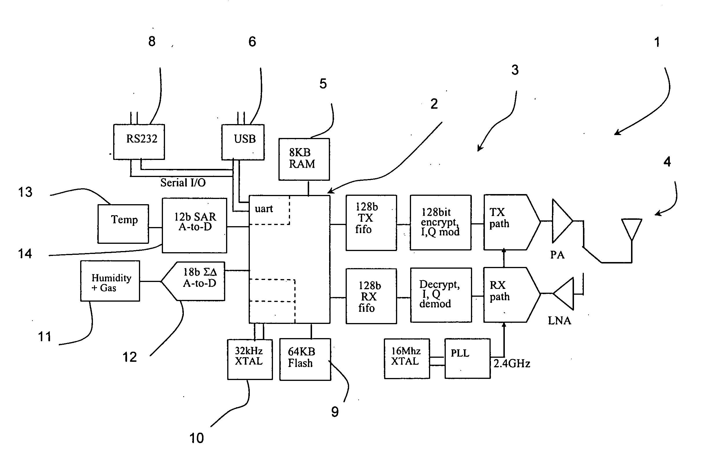
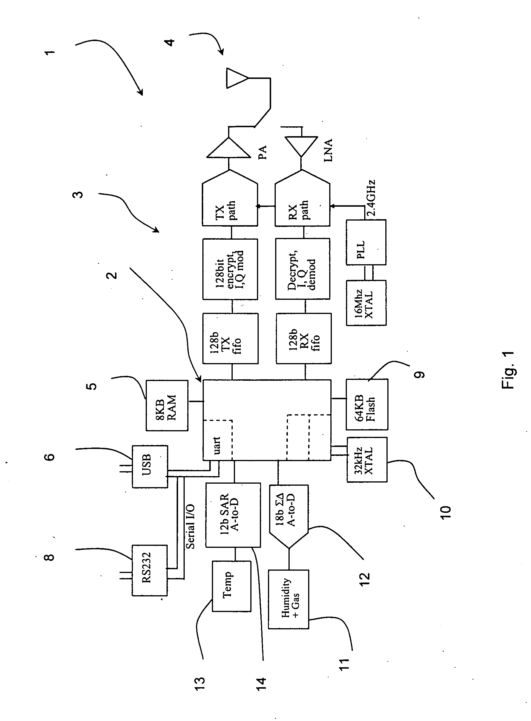
[0067] Referring to FIG. 1 a single chip wireless sensor 1 comprises a microcontroller 2 connected by a transmit / receive interface 3 to a wireless antenna 4. The microcontroller 2 is also connected to an 8 kB RAM 5, a USB interface 6, an RS232 interface 8, 64 kB flash memory 9, and a 32 kHz crystal 10. In this embodiment, the device 1 senses humidity and temperature, and a humidity sensor 11 is connected by an 18 bit ΣΔ A-to-D converter 12 to the microcontroller 2 and a temperature sensor 13 is connected by a 12 bit SAR A-to-D converter 14 to the microcontroller 2.

[0068] The device 1 is a single integrated chip manufactured in a single process in which both the electronics and sensor components are manufactured using standard CMOS processing techniques, applied to achieve both electronic and sensing components in an integrated process.

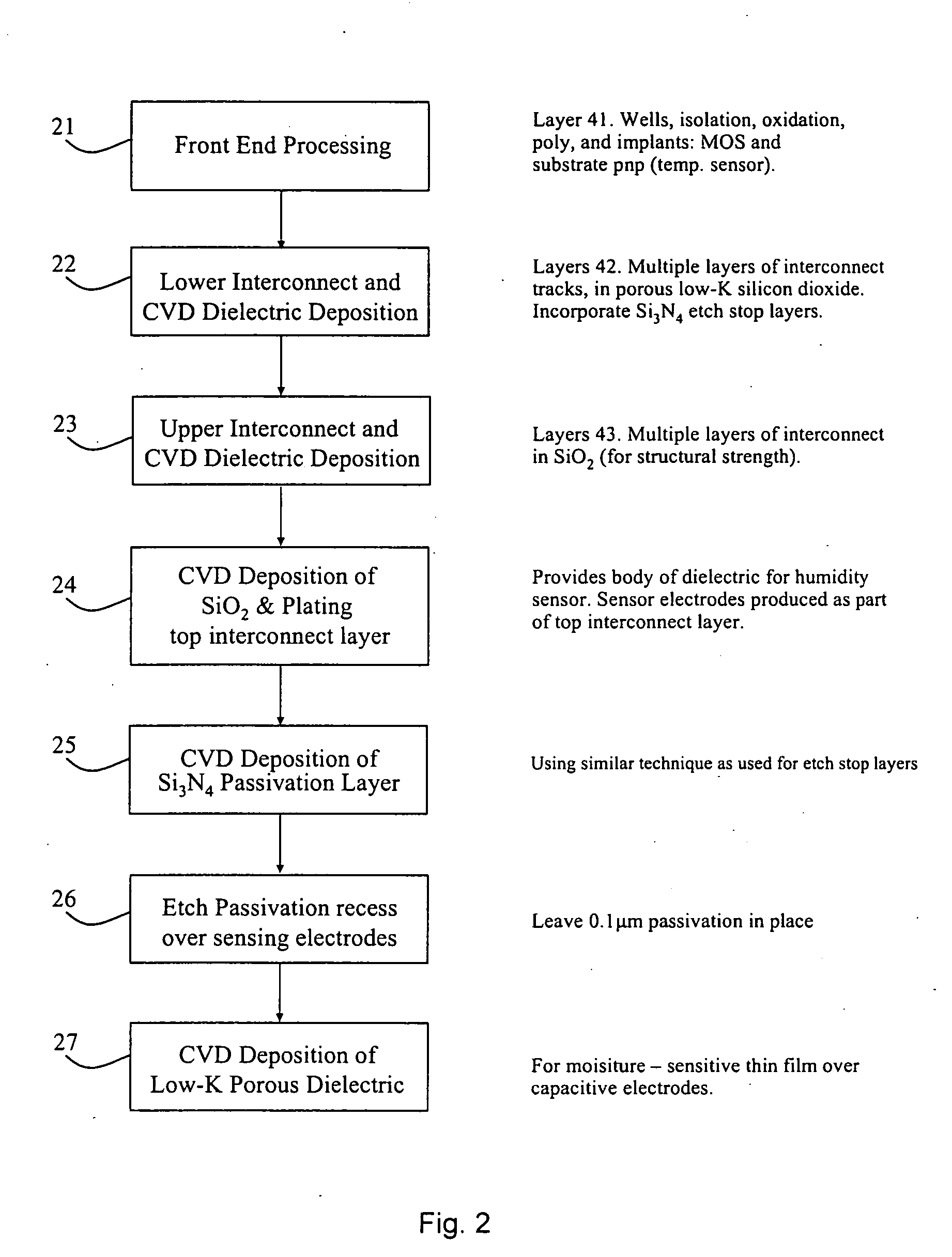
[0069] The manufacturing process 20 is now described in more detail referring to FIGS. 2, 3(a), 3(b) and 3(c), and th...


PUM


Abstract

A single chip wireless sensor (1) comprises a microcontroller (2) connected by a transmit/receive interface (3) to a wireless antenna (4). The microcontroller (2) is also connected to an 8 kB RAM (5), a USB interface (6), an RS232 interface (8), 64kB flash memory (9), and a 32 kHz crystal (10). The device (1) senses humidity and temperature, and a humidity sensor (11) is connected by an 18 bit ΣΔ A-to-D converter (12) to the microcontroller (2) and a temperature sensor (13) is connected by a 12 bit SAR A-to-D converter (14) to the microcontroller (2). The device (1) is an integrated chip manufactured in a single process in which both the electronics and sensor components are manufactured using standard CMOS processing techniques, applied to achieve both electronic and sensing components in an integrated process.

Description

FIELD OF THE INVENTION [0001] The invention relates to electronic sensors. PRIOR ART DISCUSSION [0002] One of the main driving forces in the electronics industry is the desire to achieve greater integration of functionality so that production is more automated and per-unit cost reduced. An added benefit is, of course, decreased size and thus higher circuit density. Most importantly, for battery applications, higher integration generally results in lower power, due to reduced parasitic capacitances. [0003] However in the field of sensors, and in particular wireless sensors, greater integration has been slow because of the difficulties encountered in integration of microcontroller, A-to-D converter (ADC), memory, RF transceiver, and sensor elements in the one integrated sensor device. These difficulties have arisen because of incompatibilities of materials processing for the various elements. For example, sensor elements have conventionally been manufactured on ceramic or glass substr...

Claims


Application Information

Patent Timeline
IPC IPC(8): G01N27/12G01N27/22G01N27/414H01L21/469H01L23/52H01L27/105H01L27/15
CPCG01N27/121G01N27/223H01L27/105H01L27/15H01L2924/0002H01L2924/00G01N27/22H01L27/0629H01L23/528
Inventor CUMMINS, TIMOTHY
Owner SILICON LAB INC
Why Eureka
Try Eureka