Lowpass filter formed in a multi-layer ceramic
a lowpass filter and multi-layer ceramic technology, applied in the field of elliptic lowpass filters, can solve the problems of requiring additional inductors, requiring additional inductors, and affecting the performance of lowpass filters, so as to reduce the overall area of the lowpass filter, improve the stopband rejection, and reduce the effect of circuit area
- Summary
- Abstract
- Description
- Claims
- Application Information
AI Technical Summary
Benefits of technology
Problems solved by technology
Method used
Image
Examples
first embodiment
[0038] Please refer to FIG. 6 and FIG. 7. FIG. 6 is a circuit model of a third-order filter 50 according to the present invention. FIG. 7 is a perspective diagram showing the third-order filter 50 realized in a multi-layered substrate with a bottom ground plane according to the present invention. A total of four layers are shown plus the ground plane. On layer 4, inductor L1 is formed out of a spiral inductor 52 that may be made out of a spiral metal strip. One end of the spiral inductor 52 is connected to port P1 and the other end of the spiral inductor 52 is connected to a contact node 54. The contact node 54 connects the spiral inductor 52 to a via 56 that extends from layer 1 to layer 4. On layer 3, inductor L3 is formed out of a spiral inductor 60. The spiral inductor 60 is connected between port P2 at one end and to the via 56 through a contact node 58 at the other end. Capacitor C2 is formed between layer 2 and the ground plane. Layer 2 contains a metal plate 62 with a hole 6...
second embodiment
[0041] Please refer to FIG. 9. FIG. 9 is a perspective diagram of a third-order filter 72 according to the present invention. The third-order filter 72 is similar to the third-order filter 50 of FIG. 7 except the capacitor C2 of the third-order filter 72 is formed on only one layer, which is layer 1. Because the capacitor C2 is formed on only one layer, the third-order filter 72 can be built using one less layer than the third-order filter 50 of FIG. 7.
third embodiment
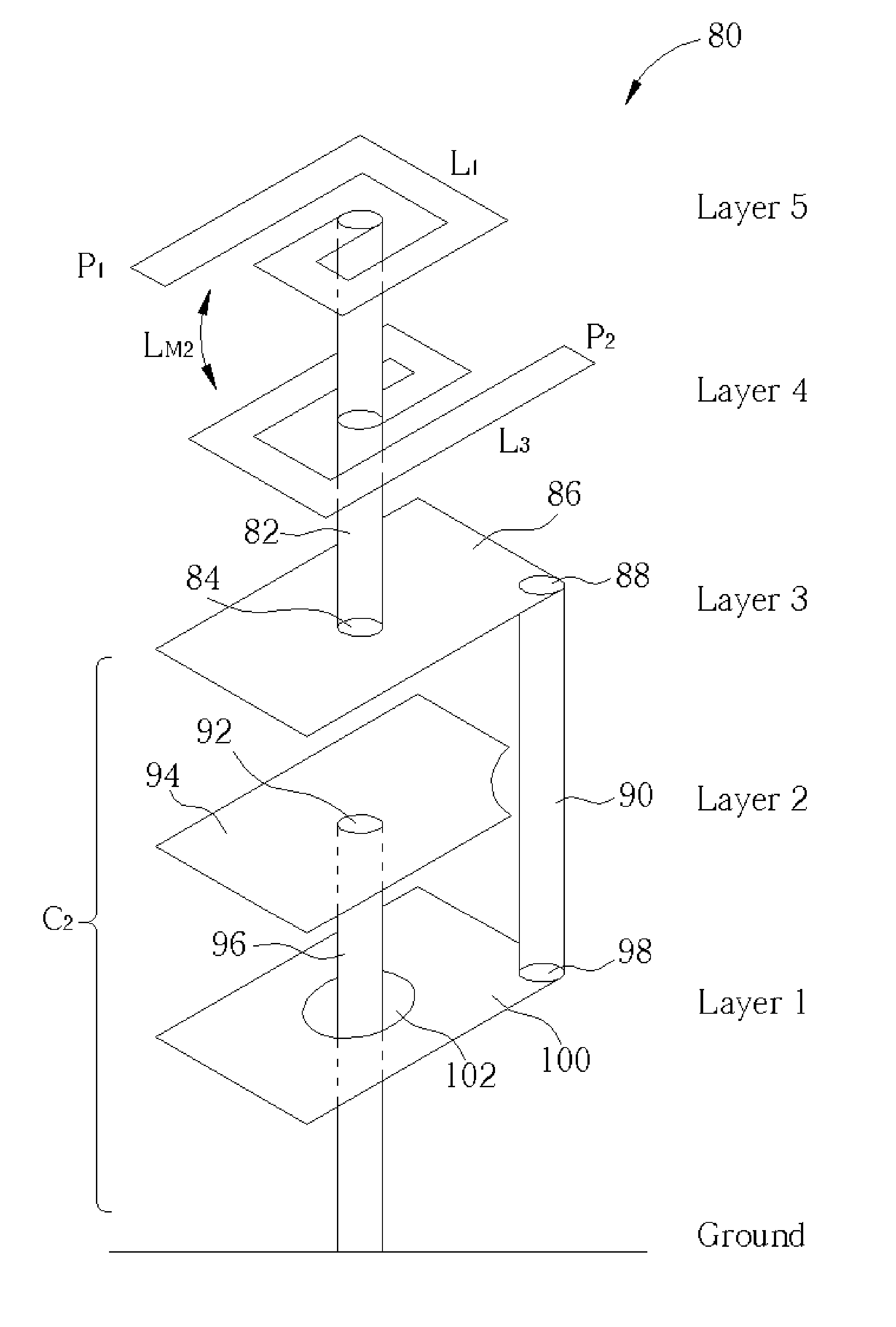
[0042] Please refer to FIG. 10. FIG. 10 is a perspective diagram showing a third-order filter 80 realized in a multi-layered substrate according to the present invention. The third-order filter 80 is realized in a total of five layers plus the ground plane. Layers 4 and 5 of the third-order filter 80 are exactly the same as layers 3 and 4 of the third-order filter 50 shown in FIG. 7. Instead of using two layers containing metal sheets to form capacitor C2, the third-order filter 80 forms the capacitor C2 out of three layers of metal sheets. On layer3, a metal sheet 86 connects to a via 82 at contact node 84. The metal sheet 86 connects to another via 90 at contact node 88. The via 90 serves to connect the metal sheet 86 on layer 3 to a metal sheet 100 on layer 1 through contact node 98. Therefore, the metal sheet 86 is electrically connected to the metal sheet 100 for providing a larger effective capacitive area. Another metal sheet 94 is formed on layer 2, and is connected to via 9...
PUM
| Property | Measurement | Unit |
|---|---|---|
| mutual inductance | aaaaa | aaaaa |
| frequencies | aaaaa | aaaaa |
| insertion losses | aaaaa | aaaaa |
Abstract
Description
Claims
Application Information


