Method of forming metal wiring of semiconductor device

a technology of metal wiring and semiconductor devices, applied in pisciculture, aquaria, marine site engineering, etc., can solve the problem of step coverage degradation of anti-diffusion film

Active Publication Date: 2005-10-06
MAGNACHIP SEMICONDUCTOR LTD
View PDF9 Cites 2 Cited by
  • Summary
  • Abstract
  • Description
  • Claims
  • Application Information

AI Technical Summary

Benefits of technology

[0006] Accordingly, the present invention has been made in view of the above problems, and it is an object of the present invention to provide a method of forming a me

Problems solved by technology

Thus, there is a problem in that the step coverage of the anti-

Method used


Image

  • Method of forming metal wiring of semiconductor device
  • Method of forming metal wiring of semiconductor device
  • Method of forming metal wiring of semiconductor device

Examples


Embodiment Construction

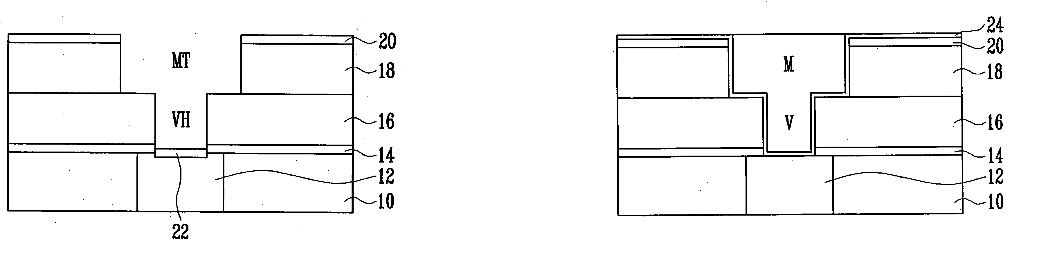
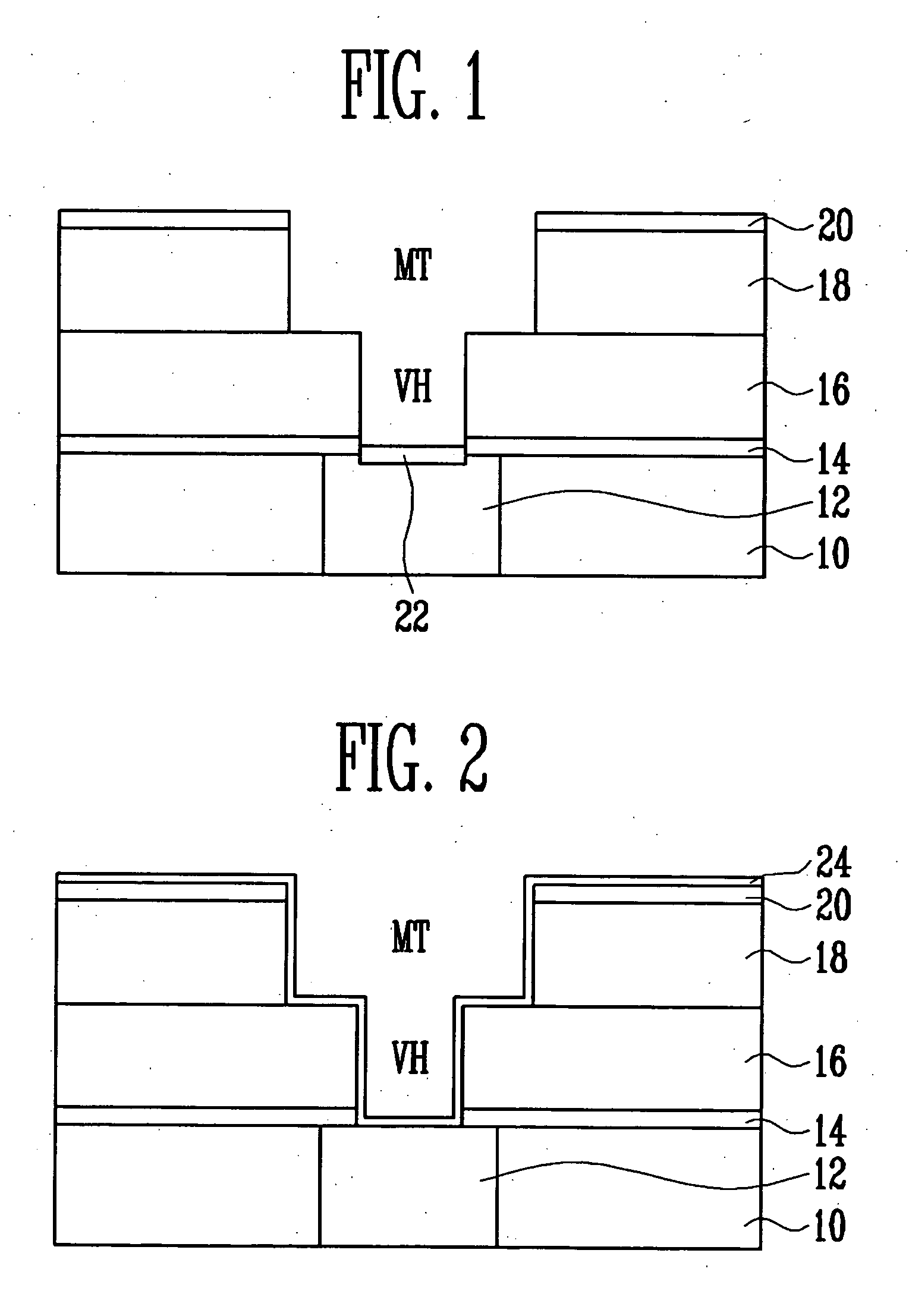
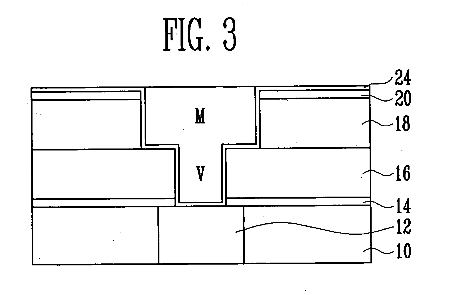
[0014] Now, the preferred embodiments according to the present invention will be described with reference to the accompanying drawings. Since preferred embodiments are provided for the purpose that the ordinary skilled in the art are able to understand the present invention, they may be modified in various manners and the scope of the present invention is not limited by the preferred embodiments described later. Further, in the drawing, the thickness and size of each layer are exaggerated for explanation's convenience and clarity. Like reference numerals are used to identify the same or similar parts. Meanwhile, in case where it is described that one film is “on” the other film or a semiconductor substrate, the one film may directly contact the other film or the semiconductor substrate. Or, a third film may be intervened between the one film and the other film or the semiconductor substrate.

[0015] FIGS. 1 to 3 are cross-sectional views for explaining a method of forming a metal wir...


PUM


Abstract

Disclosed herein is a method of forming a metal wiring of a semiconductor device. A method of forming a metal wiring of a semiconductor device comprises the steps of sequentially forming a first anti-diffusion film, a second interlayer insulating film, a third interlayer insulating film and a capping film on a first interlayer insulating film in which a first metal wiring is formed, patterning the capping film, the third interlayer insulating film, the second interlayer insulating film and the first anti-diffusion film so that the first metal wiring is exposed, thus forming a via hole, patterning the capping film and the third interlayer insulating film so that a given surface of the second interlayer insulating film is exposed on the result in which the via hole is formed, thus forming a metal wiring trench, forming a second anti-diffusion film in the via hole and the metal wiring trench, and sequentially forming copper seed layers in the via hole and the metal wiring trench in which the second anti-diffusion film is formed, and then forming a copper layer by means of an electroplating process, thus forming a via and a metal wiring.

Description

BACKGROUND [0001] 1. Field of the Invention [0002] The present invention relates to a method of forming a metal wiring of a semiconductor device, and more specifically, to a method of forming a metal wiring of a semiconductor device, which is formed by a dual damascene process. [0003] 2. Discussion of Related Art [0004] Generally, upon formation process of a metal wiring of a semiconductor device, an anti-diffusion film formation process serves to form an anti-diffusion film in a via hole and on a sidewall of a metal wiring trench, thus preventing diffusion of a metal material, which will be formed in a subsequent process. [0005] However, the anti-diffusion film is usually formed by a sputtering process employing high-density metal plasma. In this time, deposited metal ions are deposited on the via hole and the metal wiring trench with straightness. Thus, there is a problem in that the step coverage of the anti-diffusion film is degraded as a design rule of a device reduces. SUMMARY...

Claims


Application Information

Patent Timeline
IPC IPC(8): H01L21/285H01L21/3205H01L21/4763H01L21/768
CPCH01L21/2855H01L21/76843E02B3/14E02B3/129A01K61/10
Inventor KIM, DONG JOON
Owner MAGNACHIP SEMICONDUCTOR LTD
Why Eureka
Try Eureka