
Method of fabricating an optoelectronic device having a bulk heterojunction

a heterojunction and optoelectronic technology, applied in the direction of organic semiconductor devices, final product manufacturing, sustainable manufacturing/processing, etc., can solve the problems of high cost of electrical power produced per unit area, difficult and expensive production, and low efficiency of crystalline-based devices, etc., to achieve acceptable quantum yield and power conversion efficiency

Active Publication Date: 2005-10-13
THE TRUSTEES FOR PRINCETON UNIV
View PDF26 Cites 74 Cited by
  • Summary
  • Abstract
  • Description
  • Claims
  • Application Information

AI Technical Summary

Benefits of technology

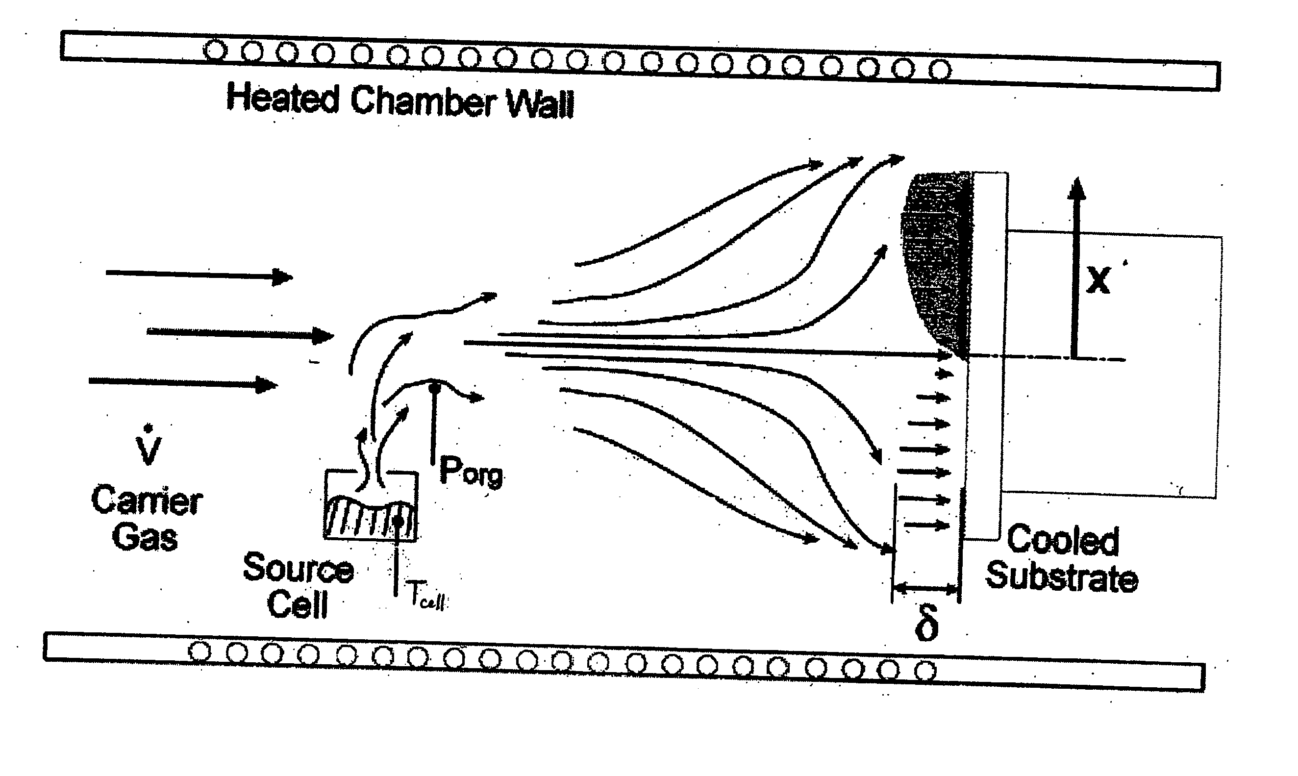
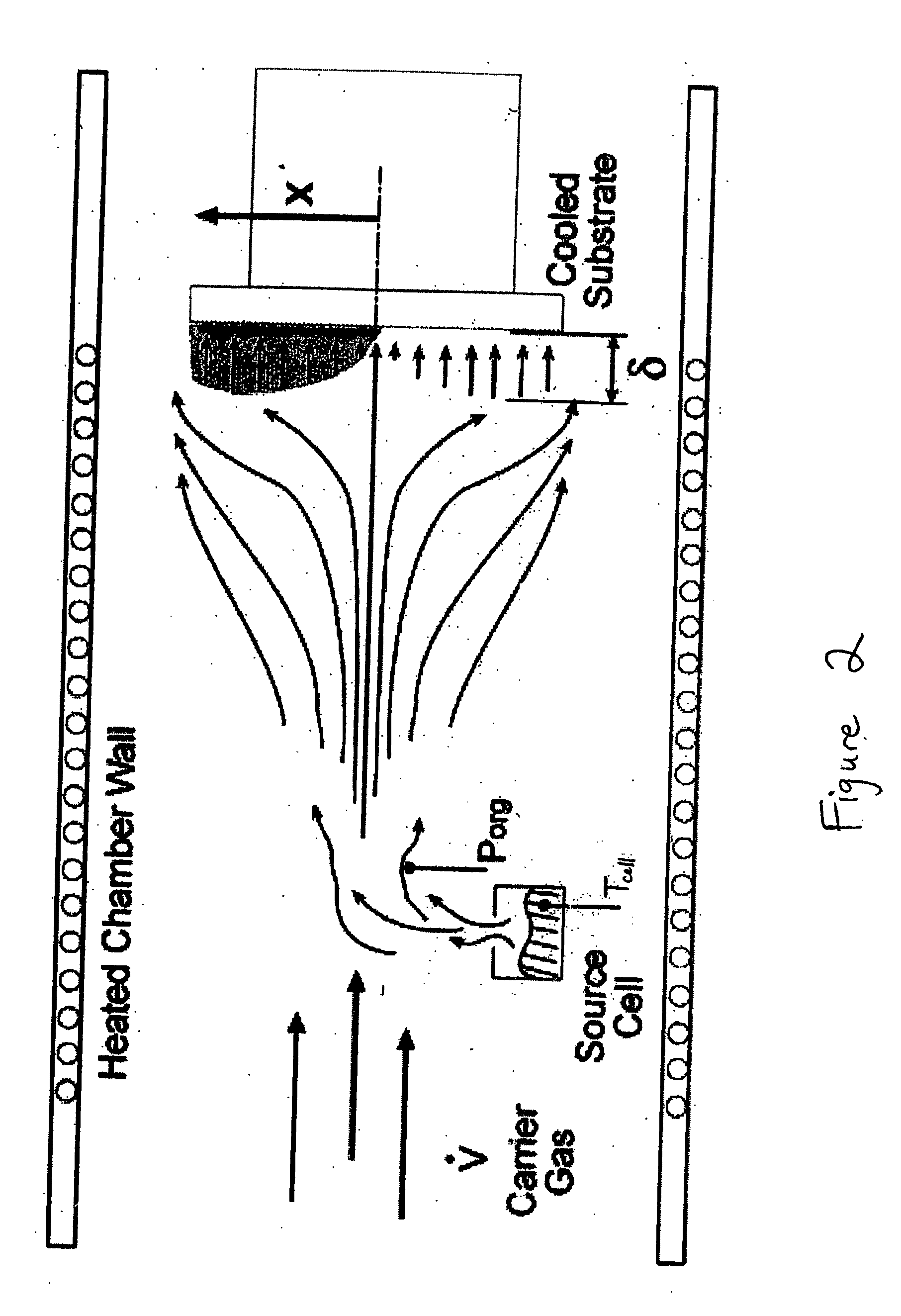
[0017] It is an object of the present invention to provide a method for the fabrication of an optoelectronic device including a bulk heterojunction, wherein the method is conducive to continuous and so-called “roll-to-roll” manufacturing techniques, and results in optoelectronic devices having acceptable quantum yields and power conversion efficiencies.

Problems solved by technology

However, efficient crystalline-based devices, especially of large surface area, are difficult and expensive to produce due to the problems inherent in producing large crystals without significant efficiency-degrading defects.
On the other hand, high efficiency amorphous silicon devices still suffer from problems with stability.
Due to the manufacturing and stability issues associated with crystalline or amorphous silicon devices, the cost of the electrical power produced per unit area has been high.
The use of current inorganic solar cells is currently limited by their high manufacturing costs relative to the electrical power produced per unit area, as well as their high installation costs resulting from the cumbersome nature of the cell frames, the remainder of system equipment, and the panels themselves.

Method used


Image

  • Method of fabricating an optoelectronic device having a bulk heterojunction
  • Method of fabricating an optoelectronic device having a bulk heterojunction
  • Method of fabricating an optoelectronic device having a bulk heterojunction

Examples


example 1

[0086] Organic vapor phase deposition was employed to deposit CuPc (an electron donor material) on silicon (a substrate) at an underlying substrate temperature of about 60° C. The deposited layer of CuPc had a high surface area-to-volume ratio, as can be seen in the scanning electron micrograph shown in FIG. 3(a).

example 2

[0087] Organic vapor phase deposition was employed to deposit CuPc (an electron donor material) on silicon (a substrate) at an underlying substrate temperature of about 100° C. The deposited layer of CuPc had a high surface area-to-volume ratio, as can be seen in the scanning electron micrograph shown in FIG. 3(b).

example 3

[0088] Organic vapor phase deposition was employed to deposit CuPc (an electron donor material) on indium-tin-oxide (an electrode) at an underlying substrate temperature of about 100° C. The deposited layer of CuPc had a high surface area-to-volume ratio, as can be seen in the scanning electron micrograph shown in FIG. 3(c).


PUM


Abstract

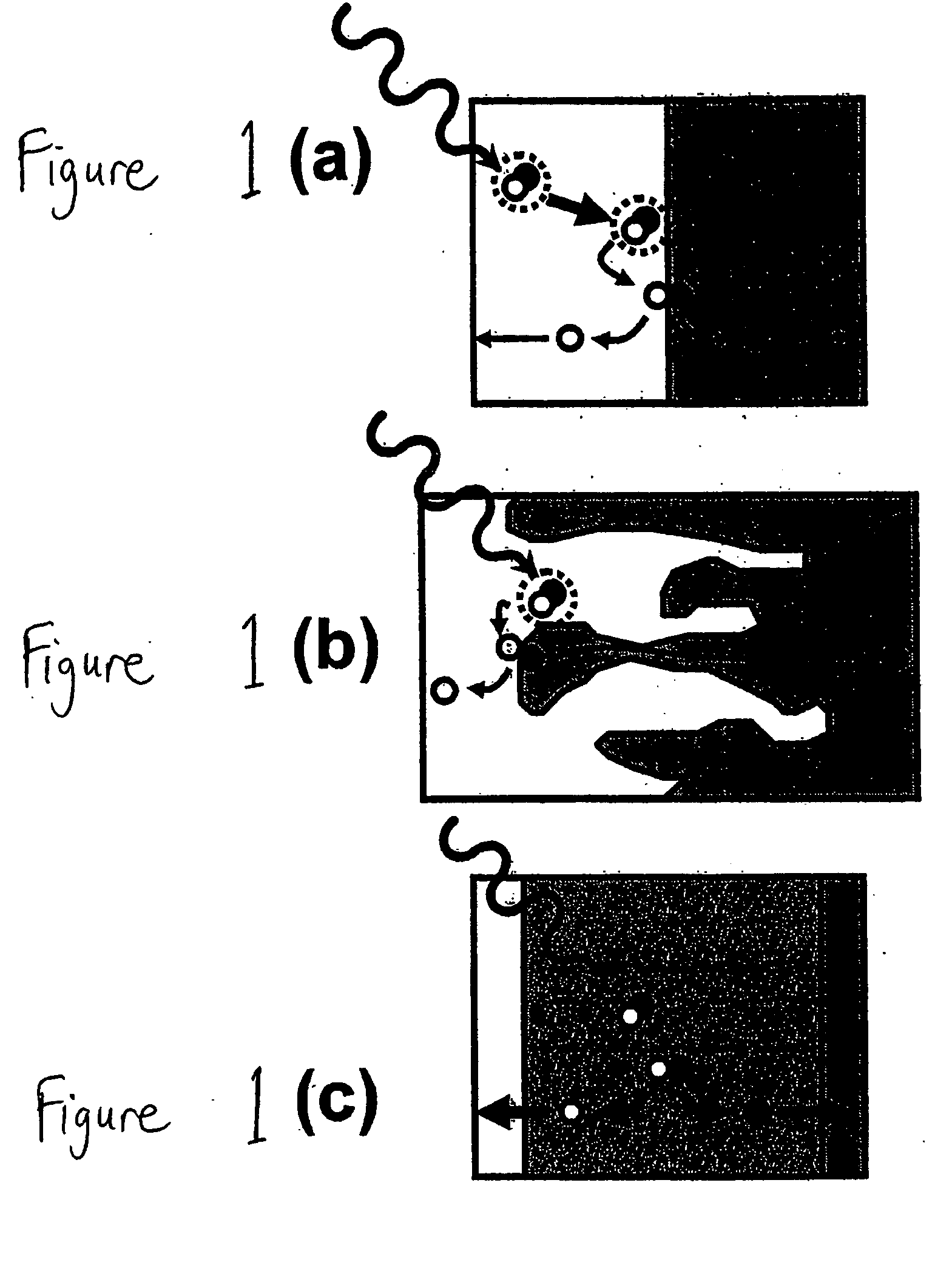
A method of fabricating an optoelectronic device comprises: depositing a first layer having protrusions over a first electrode, in which the first layer comprises a first organic small molecule material; depositing a second layer on the first layer such that the second layer is in physical contact with the first layer; in which the smallest lateral dimension of the protrusions are between 1 to 5 times the exciton diffusion length of the first organic small molecule material; and depositing a second electrode over the second layer to form the optoelectronic device. A method of fabricating an organic optoelectronic device having a bulk heterojunction is also provided and comprises: depositing a first layer with protrusions over an electrode by organic vapor phase deposition; depositing a second layer on the first layer where the interface of the first and second layers forms a bulk heterojunction; and depositing another electrode over the second layer.

Description

[0001] This application is a continuation-in-part of U.S. application Ser. No. 10 / 824,288, filed Apr. 13, 2003 entitled Method of Fabricating an Optoelectronic Device Having a Bulk Heterojunction, and which is incorporated by reference in its entirety.FIELD OF THE INVENTION [0002] The present invention generally relates to a method of fabricating an optoelectronic device. More specifically, it is directed to a method of fabricating an optoelectronic device including a bulk heterojunction. BACKGROUND [0003] Optoelectronic devices rely on the optical and electronic properties of materials to either produce or detect electromagnetic radiation electronically or to generate electricity from ambient electromagnetic radiation. Photosensitive optoelectronic devices convert electromagnetic radiation into electricity. Photovoltaic (PV) devices or solar cells, which are a type of photosensitive optoelectronic device, are specifically used to generate electrical power. PV devices, which may gen...

Claims


Application Information

Patent Timeline
IPC IPC(8): H01L29/06H01L51/00H01L51/42
CPCB82Y30/00H01L51/0008H01L51/0053H01L51/0078Y02E10/549H01L51/4246H01L51/4253H01L2251/308H01L51/4213Y02P70/50H10K71/16H10K85/621H10K85/311H10K30/211H10K30/10H10K30/30H10K2102/103H10K30/50
Inventor SHTEIN, MAXYANG, FANFORREST, STEPHEN R.
Owner THE TRUSTEES FOR PRINCETON UNIV
Learn More