Wing gate transistor for integrated circuits

Inactive Publication Date: 2005-10-13
CHARTERED SEMICONDUCTOR MANUFACTURING
View PDF5 Cites 2 Cited by
  • Summary
  • Abstract
  • Description
  • Claims
  • Application Information

AI Technical Summary

Benefits of technology

[0011] The present invention provides a system for forming a semiconductor device. Layers of gate dielectric material, gate material, and cap material are formed on a semiconductor substrate. The cap material and a portion of the gate material are processed to form a cap and a gate body portion. A wing on the gate body portion is formed from a remaining portion of the gate material. The gate dielectric material under a portion of the wing on the gate body portion is removed to form a gate dielectric. A lightly-doped source / drain is formed in the semiconductor substrate using the gate body portion and the wing. The present invention permits shrinking of transistors while improving punch-through performance, threshold voltage roll-off, and other short-channel effects.

Problems solved by technology

However, as the size of the transistor is reduced, the punch-through performance, threshold voltage roll-off, and other short channel effects become problematic.
Moreover, for short-channel devices, the threshold voltage and leakages are reaching the point where the transistors would not be operational.
Solutions to these problems have been long sought, but have also long eluded those skilled in the art.

Method used


Image

  • Wing gate transistor for integrated circuits
  • Wing gate transistor for integrated circuits
  • Wing gate transistor for integrated circuits

Examples


Embodiment Construction

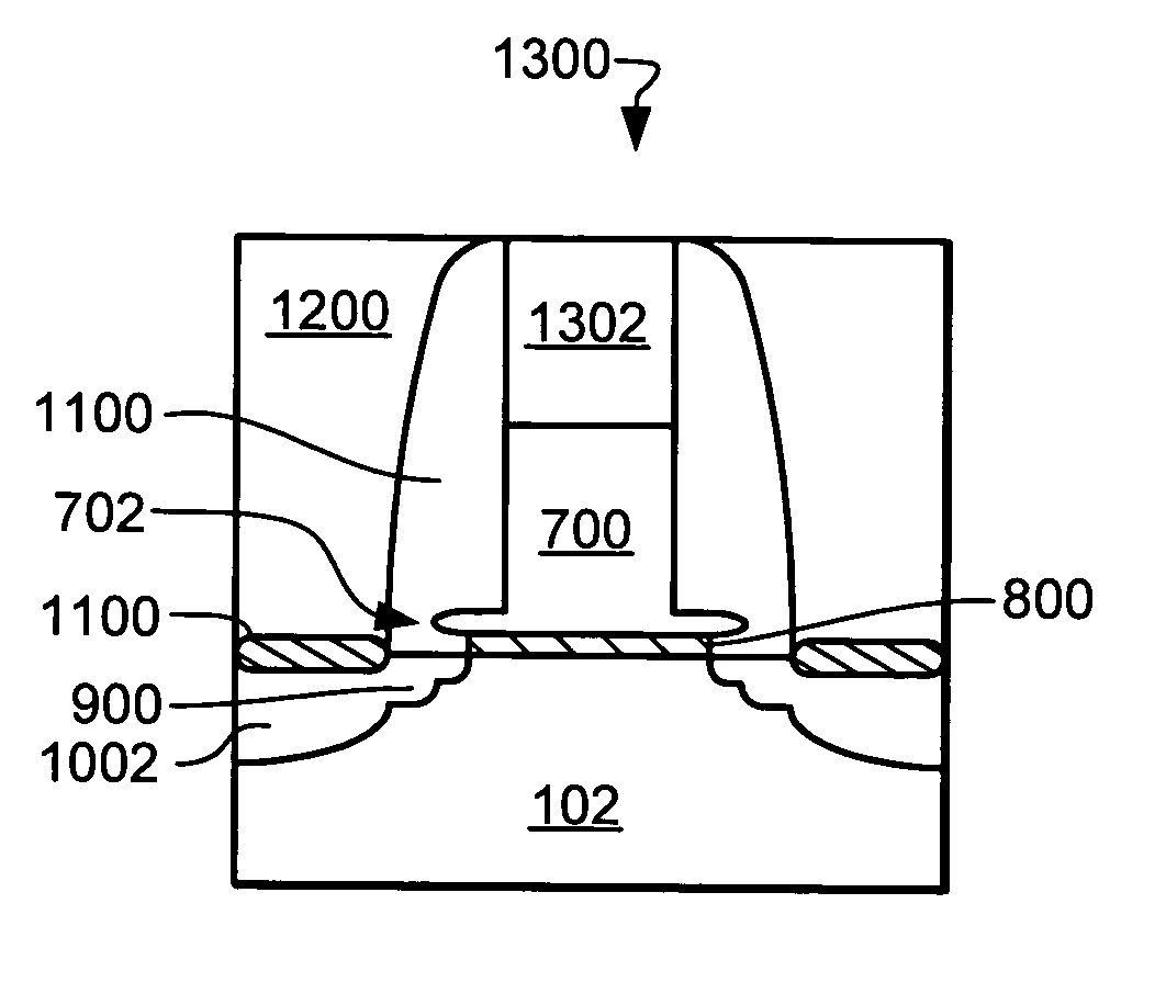
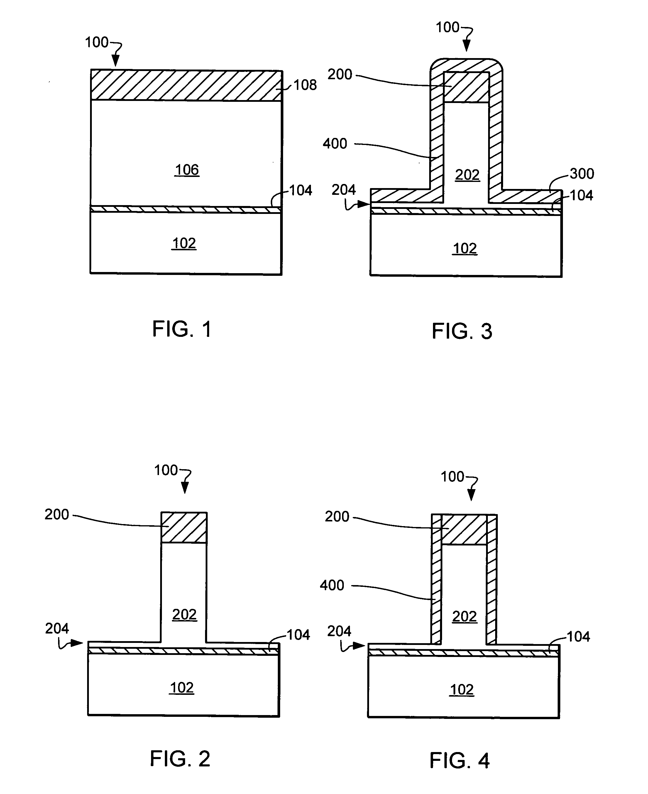
[0027] Referring now to FIG. 1, therein is shown a semiconductor device 100, such as a transistor, in an intermediate stage of manufacture. A well has been formed in a semiconductor substrate 102, such as a silicon substrate, and processing performed to form a gate dielectric layer 104, such as a silicon dioxide or nitrided oxide. A gate material layer 106, such as amorphous or polycrystalline silicon, has been deposited on the gate dielectric layer 104, and a cap material layer 108, such as nitride, has been deposited on the gate material layer 106.

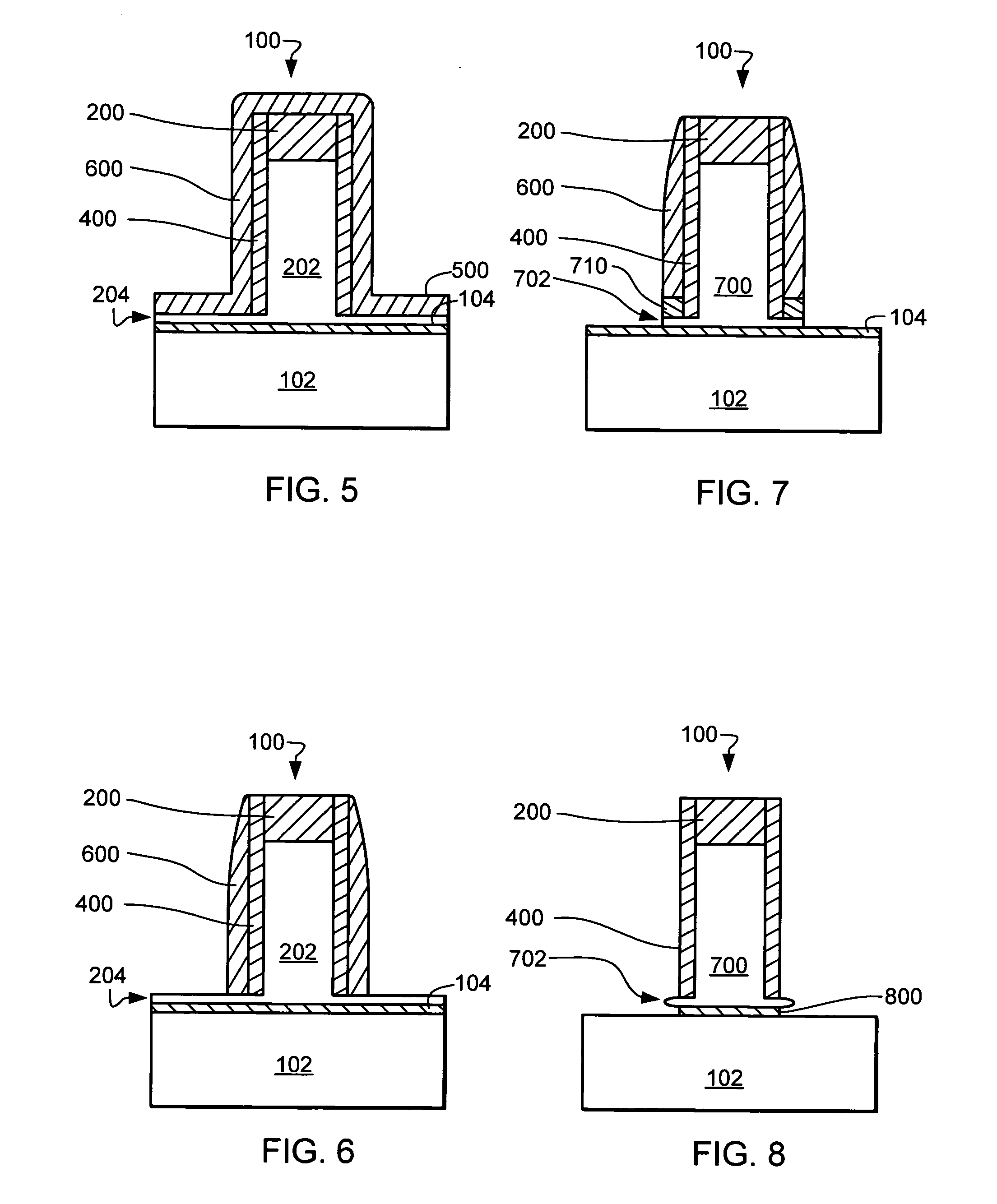
[0028] The drawings showing embodiments of the invention are semi-diagrammatic and not to scale and, particularly, some of the dimensions are for the clarity of presentation and are shown greatly exaggerated in the FIGs. In addition, where multiple embodiments are disclosed and described having some features in common, for clarity and ease of illustration and description thereof like features one to another will ordinarily be described ...


PUM


Abstract

A system is provided for forming a semiconductor device. Layers of gate dielectric material, gate material, and cap material are formed on a semiconductor substrate. The cap material and a portion of the gate material are processed to form a cap and a gate body portion. A wing on the gate body portion is formed from a remaining portion of the gate material. The gate dielectric material under a portion of the wing on the gate body portion is removed to form a gate dielectric. A lightly-doped source / drain region is formed in the semiconductor substrate using the gate body portion and the wing.

Description

BACKGROUND [0001] 1. Field of the Invention [0002] The present invention relates generally to integrated circuits, and more particularly to reduced-size transistors. [0003] 2. Background of the Invention [0004] The present invention relates generally to electronics and more particularly to electronic components. [0005] Semiconductor devices such as transistors, are formed in and upon semiconductor substrates. These circuit elements are interconnected by contacts and vias, which connect to patterned conductor layers which are separated by various dielectric layers. [0006] A critical objective of the semiconductor industry has been to continually decrease the size of semiconductor devices to increase performance and reduce cost for applications such as cellphones and portable CD players. As semiconductor technology has advanced, there has been a continuing concentration on reducing the size of the semiconductor devices to allow for increased levels of circuit integration, improved per...

Claims


Application Information

Patent Timeline
IPC IPC(8): H01L21/28H01L21/336H01L21/338H01L27/148H01L29/423H01L29/74H01L29/76H01L29/768H01L29/78H01L29/94H01L31/062H01L31/113H01L31/119
CPCH01L21/28114H01L29/42376H01L29/665H01L29/7833H01L29/6656H01L29/6659H01L29/6653
Inventor PHUA, TIMOTHYTEE, KHENG CHOKHSIA, LIANG CHOO
Owner CHARTERED SEMICONDUCTOR MANUFACTURING
Why Eureka
Try Eureka