Methods of making, positioning and orienting nanostructures, nanostructure arrays and nanostructure devices

a nanostructure and array technology, applied in the field of nanostructures, can solve the problems of insufficient current technologies to form high yields of nanostructures, cumbersome arrays and functional devices, and insufficient methods of assembling nanostructures into junctions

Inactive Publication Date: 2005-10-20
ONED MATERIAL INC
View PDF45 Cites 112 Cited by
  • Summary
  • Abstract
  • Description
  • Claims
  • Application Information

AI Technical Summary

Benefits of technology

[0012] In light of the present invention, it will be apparent to one of skill in the art that one can create a patterned array of nanostructure catalysts with an almost unlimited set of parameters. These parameters can include the size and shape of each individual patterned element, the thickness of each individual patterned element, the material from which each individual patterned element is formed (e.g. including but not limited to gold, iron, cobalt, manganese, alloys, etc.). It is even possible, using standard lithographic processes, to create arrays of multiple different patterned materials, each from a different material. Each of these different patterned elements can be fabricated simultaneously or sequentially. It is possible to grow nanostructures from one array of patterned elements and then add additional patterned elements to the substrate to grow a second set of nanostructures. In this case, the nanostructures of the first and second set can be made from either the same or different nanostructure precursors. It is also possible to remove any remaining catalyst / precursor spheres created in the first step prior to depositing the second set of patterned elements. This provides precise control over the material characteristics of the final nanostructure array.
[0015] In another aspect of the invention, methods of growing a nanostructure such as a nanowire in a selected direction or orientation are provided. In the methods, a magnetic field is applied to a eutectic interface between a nanostructure crystal and a catalyst mixture comprising a magnetic colloid (e.g., iron) and a nanostructure precursor. Note that the catalyst mixture may optionally comprise additional nonmetallic catalyst materials. This results in control over the direction or and diameter of nanostructure growth. By applying a force that interacts with the catalyst colloid (e.g. a magnetic field), the direction of the interface between the liquid and solid can be modified and the direction of subsequent growth affected. The nanostructure will tend to grow in a direction normal to the resulting interface. Alternatively, if the force is directed normal to the existing interface, the result will be a deformation of the catalyst colloid, increasing or decreasing the effective diameter of the resulting sphere and therefore the resulting nanostructure. In this way, the methods of the present invention can be used to intentionally modify the diameter of the nanostructure during the growth process. Note that even forces that are directed non-normal to the existing interface can optionally change the effective diameter of the sphere.
[0040] In the present invention, the magnitude of the electric field is modulated by a feedback mechanism that prevents a significant current from flowing through nanostructure after it bridges the gap between the electrodes. A change in current between the electrodes upon contact, or a change in capacitance between the electrodes during growth is detected, and the electric field is modified (e.g., reduced or turned off) in response to the nanostructure contact or the change in capacitance. In one simple embodiment, the automatic detection is performed with a circuit comprising a resistor. In another embodiment, the system comprises a current-divider, as is known in the art, such that the relative resistance of a nanostructure is substantially larger than a second conducting path that the amount of current flow across the nanostructure at the voltages used for directed growth do not cause the nanostructure to break.
[0042] Extended contact by a nanostructure such as a nanowire to both electrodes while a potential difference exists between the electrodes can be undesirable, because the flow of current through the nanowire (or other relevant nanostructure) can burn out the nanowire if the flow is to high. Thus, detection of capacitance can be used to shut the electric field off just prior to or approximately simultaneous with contact of a growing nanowire to a destination electrode. As the nanostructure grows toward the second electrode, the spacing between the electrodes decreases, and the capacitance decreases. This measurement can be calibrated as a direct measure of the remaining distance between the nanostructure and the second electrode. Alternatively, the nanostructure can be grown for a period of time known to bridge enough of the gap between electrodes that the nanostructure will continue to grow in substantially the same direction, contacting the second electrode in the absence of an electric field. That way, the electric field can be turned off in the absence of any direct feedback. Alternately, the nanostructures are grown in the presence of a gate voltage, whereby the nanostructures are rendered non-conducting. As a result, the nanostructures act as insulators and no current flows upon connection with the second electrode.
[0046] In another aspect, the present invention includes methods of depositing nanostructures such as nanowires on a substrate. In the methods, nanostructures are suspended in solution. The resulting nanostructure suspension is applied to a rotatable substrate which is rotated, thereby depositing the nanostructures on the rotating rotatable substrate. This has the advantage of radially aligning the nanostructures on the rotatable substrate. The nanostructures are optionally applied to the rotatable substrate prior to rotation of the rotatable substrate, or alternately can be applied to the rotatable substrate during rotation of the rotatable substrate. The nanostructures which are radially aligned can comprise heterostructures or homostructure nanostructures. In this embodiment, the substrate is optionally chemically functionalized to bind to the nanostructures, securing them in position once they contact the surface.

Problems solved by technology

While a variety of ways of making nanostructures are available, current technologies are largely insufficient to form high yields of nanostructures, particularly of nanostructures having pre-selected properties (e.g., uniformity).
In addition, existing methods of assembling nanostructures into junctions, arrays and functional devices are fairly cumbersome.

Method used


Image

  • Methods of making, positioning and orienting nanostructures, nanostructure arrays and nanostructure devices
  • Methods of making, positioning and orienting nanostructures, nanostructure arrays and nanostructure devices
  • Methods of making, positioning and orienting nanostructures, nanostructure arrays and nanostructure devices

Examples


Embodiment Construction

Introduction

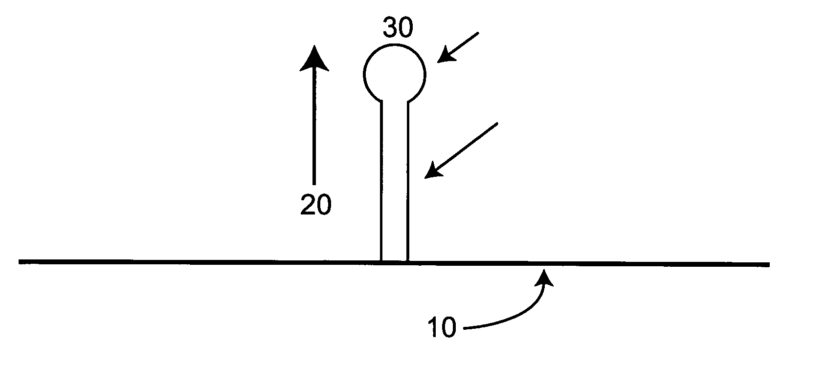
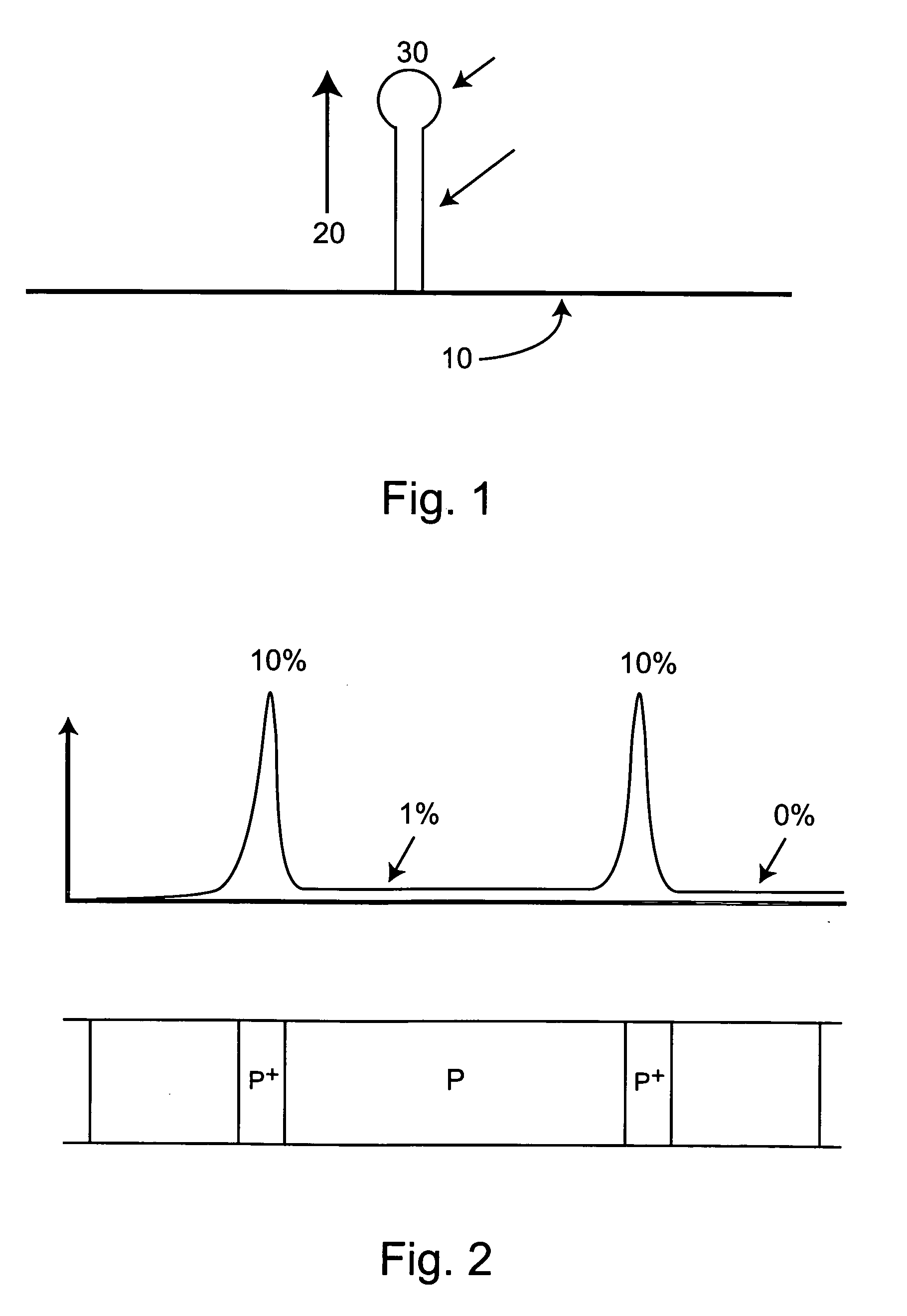
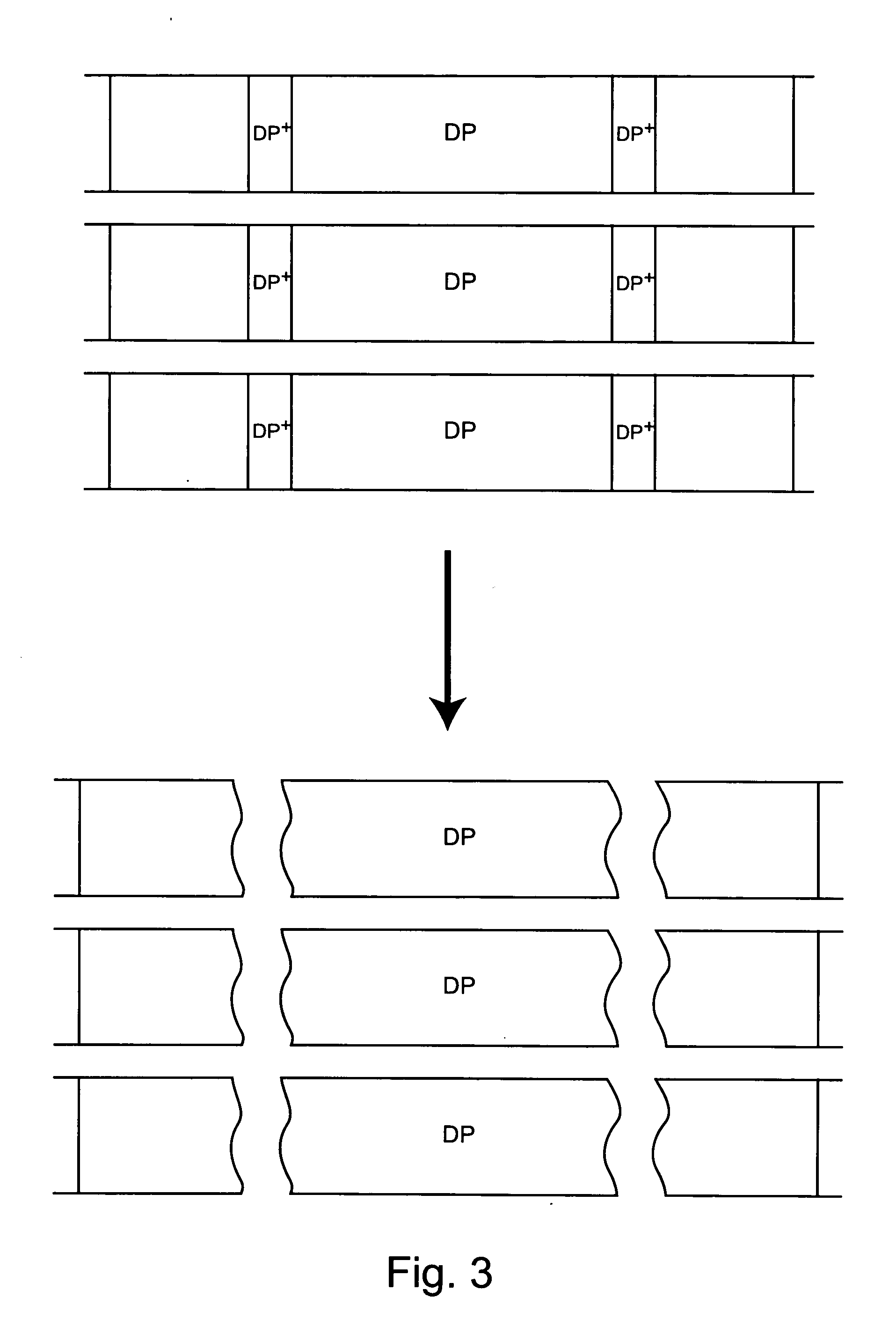
[0081] The present invention provides a variety of methods of making and arranging nanostructures such as nanowires, e.g., into functional devices, arrays or device or array components. The following discussion focuses first on the formation of nanostructures and nanostructure arrays via patterning, then focuses on oriented growth in magnetic fields and then on fluidic assembly of nanostructure arrays. Harvesting of nanostructures from a substrate via etching (including use of etch planes for making nanostructures such as nanowires with defined ends and / or controlled lengths) and manufacturing of nanostructures on substrates and integration with IC by planar processing methods is then covered. Power directed orientation and growth of nanostructures, template directed nanostructures growth and radial nanostructures deposition are addressed. Large scale growth of nanostructures, e.g., by continuous gas and plasma phase synthesis approaches are then covered, followed by n...


PUM

PropertyMeasurementUnit
thicknessaaaaaaaaaa
diameteraaaaaaaaaa
diameteraaaaaaaaaa

Abstract

Nanostructure manufacturing methods and methods for assembling nanostructures into functional elements such as junctions, arrays and devices are provided. Systems for practicing the methods are also provided.

Description

CROSS-REFERENCE TO RELATED APPLICATIONS [0001] This application is a continuation of U.S. Ser. No. 10 / 405,992, filed Apr. 1, 2003, which is a continuation-in-part of U.S. Ser. No. 10 / 239,000, filed Sep. 10, 2002, which claims the benefit of U.S. Ser. No. 60 / 370,113, filed Apr. 2, 2002. The present application claims priority to and benefit of each of these prior applications, which are hereby incorporated herein by reference in their entirety for all purposes.FIELD OF THE INVENTION [0002] This invention is in the field of nanostructure (e.g., nanowire, nanotube, nanorod, nanoribbon, quantum dot, nanodot, nanotetrapods, etc.) manufacture and assembly. BACKGROUND OF THE INVENTION [0003] In general, a hierarchy of nanostructure building block to nanostructure device exists. The basic building block of a device is the nanostructure itself, e.g., a nanowire, nanotube, nanorod, nanoribbon, quantum dot, nanodot, nanotetrapod, or the like. These structures can be semiconductors (e.g., doped...

Claims


Application Information

Patent Timeline
Patent Type & Authority Applications(United States)
IPC IPC(8): B81C99/00C23F1/00H01L51/30H01L51/40
CPCB01J23/52B81B2203/0361H01L2924/0002B81B2207/015B81C99/008B82B3/00B82Y10/00B82Y30/00B82Y40/00G11B5/743G11C2213/81H01L29/7869H01L51/0001H01L51/0048H01L51/0595Y10S977/89Y10S977/762Y10S438/962Y10S977/857Y10S977/856Y10S977/858B81C3/005B81C2203/057H01L2924/00H10K71/00H10K85/221H10K10/701
Inventor EMPEDOCLES, STEPHENBOCK, LARRYCHOW, CALVINDUAN, XIANFENGNIU, CHUNMINGPONTIS, GEORGESAHI, VIJENDRAROMANO, LINDA T.STUMBO, DAVID
Owner ONED MATERIAL INC
Why Eureka
Try Eureka