Semiconductor memory device having capacitor and method of forming the same

a memory device and capacitor technology, applied in the direction of capacitors, solid-state devices, transistors, etc., can solve the problems of difficult control of hsg formation, reduced substrate area available for capacitor formation, and reduced surface area of polycrystalline silicon, so as to increase the electrode surface area and increase the capacitance

Inactive Publication Date: 2005-10-20
SAMSUNG ELECTRONICS CO LTD
View PDF3 Cites 15 Cited by
  • Summary
  • Abstract
  • Description
  • Claims
  • Application Information

AI Technical Summary

Benefits of technology

[0009] An object of the present invention is to provide a semiconductor memory device and a method of fabricating the same, where the semiconductor memory device yields higher capacitance by forming protrusions of the bottom electrode that increase electrode surface area.
[0010] It is another object of the present invention to provide a semiconductor memory device and a method of fabricating the same, where the semiconductor memory device can prevent protrusions formed at the bottom electrode surface from becoming disjoined.

Problems solved by technology

The result is reduced substrate area available for capacitor formation.
This type of HSG formation is achieved by heat treatment and deposition, which cause the migration of silicon atoms and result in decreased surface area of the polycrystalline silicon.
However, HSG formation is difficult to control.
When this occurs, the HSG protrusion is easily disjoined, generating particles and resulting in process failure.

Method used


Image

  • Semiconductor memory device having capacitor and method of forming the same
  • Semiconductor memory device having capacitor and method of forming the same
  • Semiconductor memory device having capacitor and method of forming the same

Examples


embodiment 1

Preferred Embodiment 1

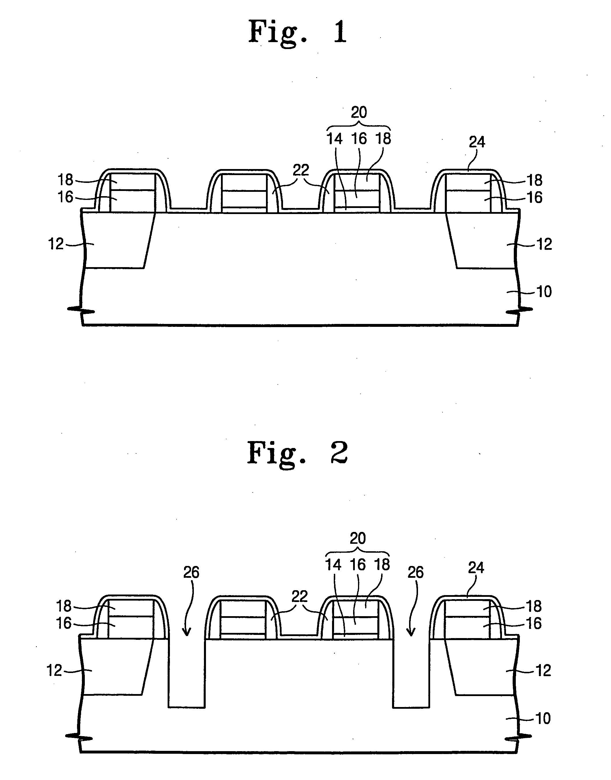
[0023] Referring to FIG. 1, a device isolation layer 12 is formed at a substrate 10. The device isolation layer 12 is formed by selectively etching the substrate 10 to form a trench. An insulation layer fills the trench. The insulation layer is formed by CVD. A gate insulation layer 14 is formed through thermal oxidation at an active region where the device isolation layer 12 is absent. A gate layer 16 and an insulation layer 18 for capping are stacked at the substrate where the gate insulation layer 14 is formed. The layers are patterned to form a gate electrode 20. Insulation spacers 22 are formed at the sidewall of the gate electrode 20. A silicon nitride layer is conformally formed as a protective layer 24 over the entire surface of the substrate.

[0024] Referring to FIG. 2, a photoresist pattern (not shown) is formed and used to remove the protective layer 24 at a desired region between the gate electrodes 20 and to expose the crystalline silicon substrate...

embodiment 2

Preferred Embodiment 2

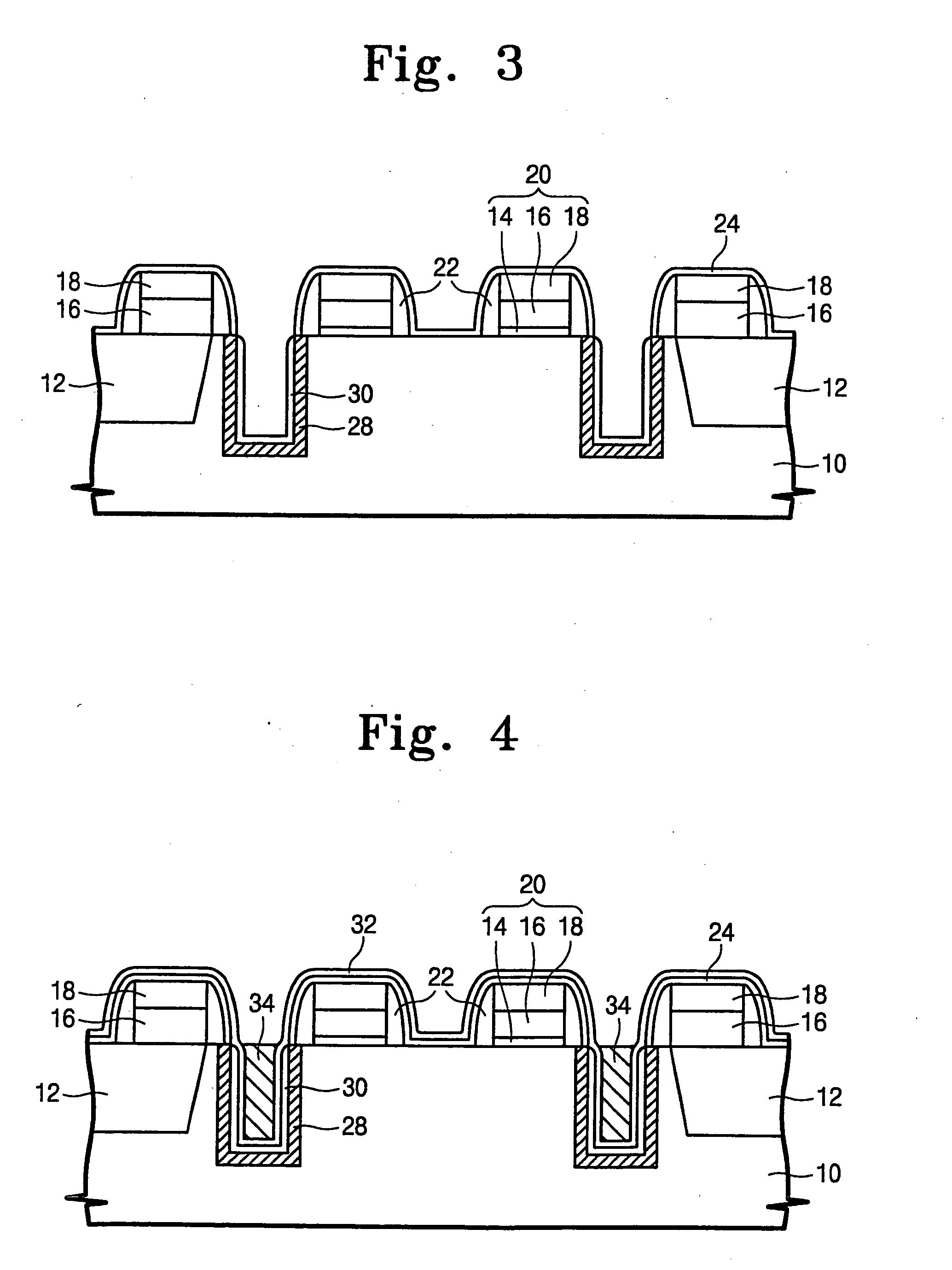
[0032]FIG. 7 is a process cross-sectional view for illustrating a capacitor bottom electrode of a semiconductor memory device in accordance with a second preferred embodiment of the present invention.

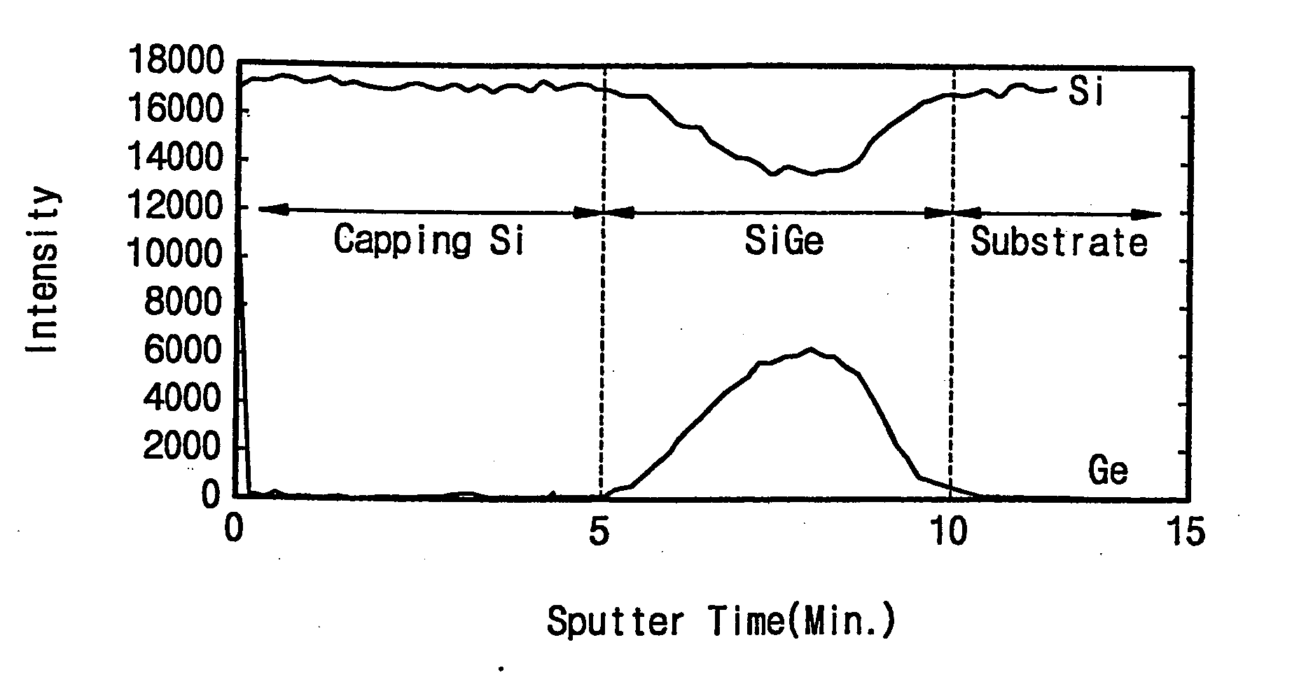
[0033] Referring to FIG. 7, the gate electrode 20, the insulation spacer 22 and the protective layer 24 are formed at the substrate 10 and the substrate 10 is exposed at a source region. Crystalline is then selectively grown where the substrate 10 is exposed. The result is the formation of a stack-type bottom electrode 36 capacitor. The surface layer 38 can be formed from a silicon germanium crystalline layer or a dual layer in which silicon crystalline is stacked on silicon germanium crystalline. A method of forming the surface layer 38 includes the following: stacking crystalline for a predefined time not to exceed 20 minutes at a pressure of approximately 20 Torr and a temperature of approximately 780° C. in a conventional LPCVD device using silane, dichlorosil...


PUM

PropertyMeasurementUnit
temperaturesaaaaaaaaaa
pressuresaaaaaaaaaa
temperatureaaaaaaaaaa

Abstract

A semiconductor memory device having a capacitor is disclosed. The capacitor includes a bottom capacitor surface formed of a silicon-germanium crystalline layer or a dual layer in which a silicon-germanium crystalline layer covers a silicon crystalline layer. The bottom capacitor surface is uneven and is conventionally formed by an epitaxial method. The silicon germanium crystalline layer is approximately 5 to 50 percent germanium content by weight. The method of fabricating the semiconductor memory device comprises: selectively exposing the surface of a crystalline silicon substrate at the region where the capacitor bottom electrode is formed; supplying a source gas to grow a silicon germanium crystalline layer at the surface of the selectively exposed silicon substrate; stacking a dielectric layer over the silicon germanium crystalline layer; and stacking a conductive layer over the dielectric layer to form a capacitor top electrode. After forming the silicon germanium crystalline layer to a predefined thickness, a silicon crystalline layer can be further grown at the silicon germanium crystalline layer. After forming the silicon germanium crystalline layer and before forming the dielectric layer, annealing can be performed for a predefined time.

Description

RELATED APPLICATION [0001] This application is a divisional of U.S. patent application Ser. No. 10 / 161,063, filed May 30, 2002, now pending, which is claims priority from Korean Patent Application No. 2001-30382, filed May 31, 2001, the contents of which are incorporated by reference.FIELD OF THE INVENTION [0002] The present invention relates to a semiconductor memory device having a capacitor and a method of fabricating the same. More particularly, the present invention relates to a semiconductor memory device having a capacitor with a higher capacitance because of increased electrode area, and to a method of fabricating the same. BACKGROUND OF THE INVENTION [0003] As semiconductor devices become more highly integrated, there is a decrease in area and wire width of individual semiconductors. The result is reduced substrate area available for capacitor formation. Conventionally, if the electrode area is decreased capacitance is also decreased. [0004] In a semiconductor memory device...

Claims


Application Information

Patent Timeline
Patent Type & Authority Applications(United States)
IPC IPC(8): H01L21/02H01L21/8242H01L27/108H01L31/0236H01L31/0745
CPCH01L27/1087H01L28/84Y02E10/50H01L31/0745H01L31/0236H01L31/02363H10B12/0387H10B12/00
Inventor PARK, JUNG-WOOHA, JUNG-MIN
Owner SAMSUNG ELECTRONICS CO LTD
Why Eureka
Try Eureka