Method for characterizing cells with consideration for bumped waveform and delay time calculation method for semiconductor integrated circuits using the same

a delay time calculation and cell technology, applied in computing, digital storage, instruments, etc., can solve problems such as deteriorating accuracy of delay time calculation, error when waveform distortion occurs, distortion of signal waveform input/output from each cell, etc., and achieve the effect of effective input terminal capacitan

Inactive Publication Date: 2005-10-20
PANASONIC CORP
View PDF4 Cites 27 Cited by
  • Summary
  • Abstract
  • Description
  • Claims
  • Application Information

AI Technical Summary

Problems solved by technology

However, there is a possibility that distortion occurs in a signal waveform input to / output from each cell according to the relationship between the driving capacity of the cell and the drive capacitance.
Nevertheless, the delay time calculation method described in IEICE Technical Report VLD98-137 fails to consider such a case and is based on the premise that no distortion occurs in the input waveform.
Thus, the calculation result includes an error when waveform distortion occurs as described above.
Especially when waveform distortion occurs in the vicinity of the threshold of delay measurement due to the above-described reason, a cell characteristic extraction result greatly differs from an actual result, and accordingly, the accuracy of delay time calculation deteriorates.
Therefore, when distortion occurs due to such a reason, the calculation result includes an error.
Further, also when the above conventional delay time calculation methods are used in a post-layout circuit modification, distortion occurs in the waveform input to / output from a cell in actuality, and therefore, the actual delay time can be longer than calculated.
In such a case, for example, an additional effort of modifying a circuit is required in a hold error correction process.
Further, the above calculation error can result in missing an error in a setup error correction process.

Method used


Image

  • Method for characterizing cells with consideration for bumped waveform and delay time calculation method for semiconductor integrated circuits using the same
  • Method for characterizing cells with consideration for bumped waveform and delay time calculation method for semiconductor integrated circuits using the same
  • Method for characterizing cells with consideration for bumped waveform and delay time calculation method for semiconductor integrated circuits using the same

Examples


embodiment 1

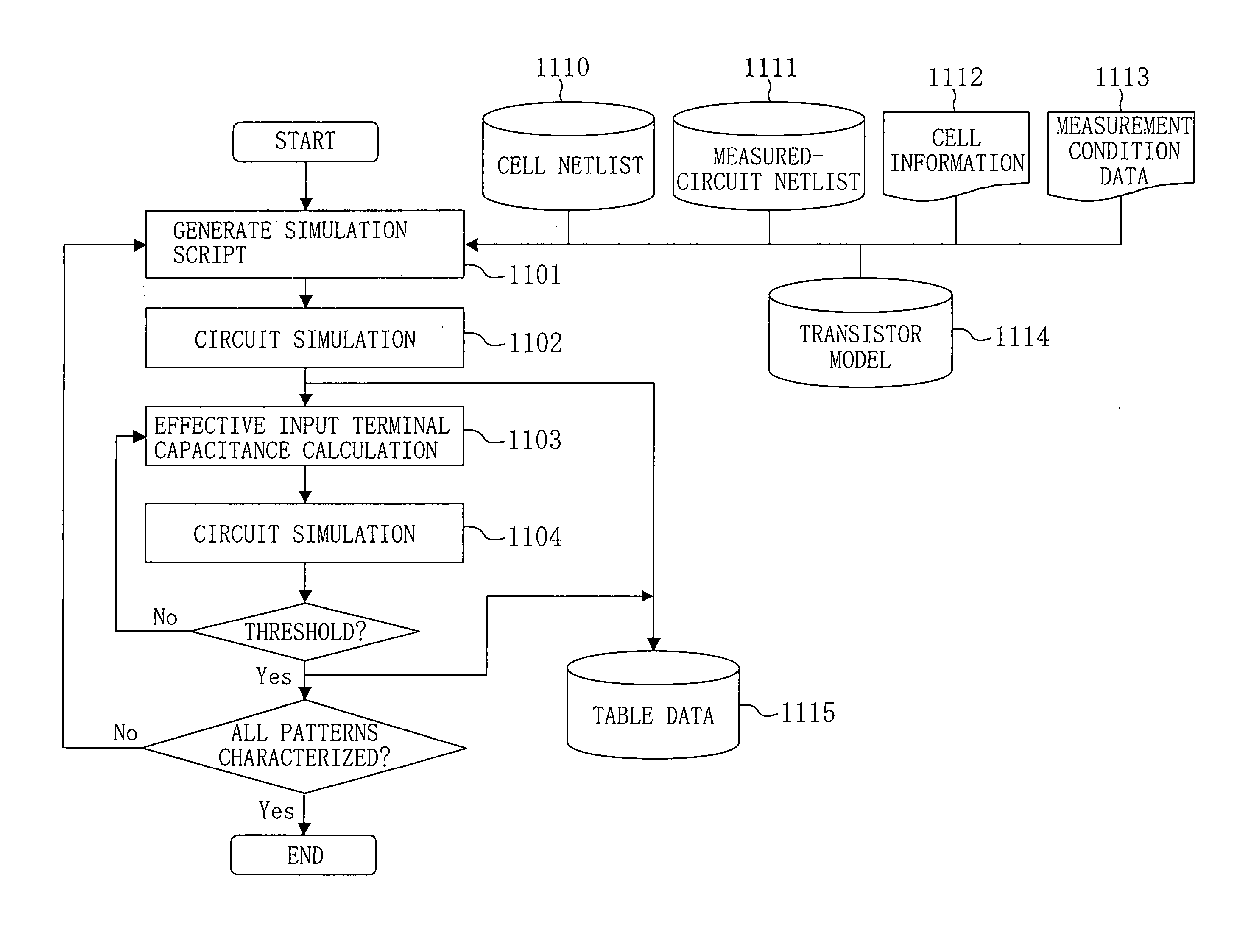
[0063] Embodiment 1 of the present invention is described with reference to FIGS. 1, 2 and 3.

[0064]FIG. 1 is a flowchart of a variable input terminal capacitance characterization method according to embodiment 1 of the present invention, in which a variation of the input terminal capacitance of a cell is considered. Embodiment 1 provides an example of a semiconductor integrated circuit formed by a large number of basic logic cells or function macroblocks (hereinafter, generically referred to as “cell(s)” for simplicity) which are connected by lines, and illustrates an example of delay time calculation with consideration for waveform distortion in each cell. In embodiment 1, a method for characterizing the characteristics of a cell is described on an assumption that waveform distortion is caused in the cell which is a delay time calculation subject circuit due to the Miller effect, and the waveform distortion causes a delay. It should be noted that, in the flowcharts of embodiment 1...

embodiment 2

[0080] Next, embodiment 2 of the present invention is described with reference to FIGS. 4, 5 and 6.

[0081]FIG. 4 is a flowchart of a bump-superimposed waveform characterization method according to embodiment 2 of the present invention. In embodiment 2, a method for characterizing the characteristics of a cell based on the characteristics of a bump waveform which is a waveform component of the distortion is described on an assumption that waveform distortion is caused in a cell (delay time calculation subject circuit) due to the Miller effect, or the like, and the waveform distortion causes a delay.

[0082]FIG. 5 shows a bump-superimposed waveform characterization circuit for generating an input waveform on which a bump is superimposed. The bump-superimposed waveform characterization circuit also measures the cell delay and the output waveform of a characterization subject cell 1404. In the example of FIG. 5, a bump (bump input waveform) generated by a bump voltage generation section ...

embodiment 3

[0091] Embodiment 3 of the present invention is described with reference to FIGS. 7, 8 and 9.

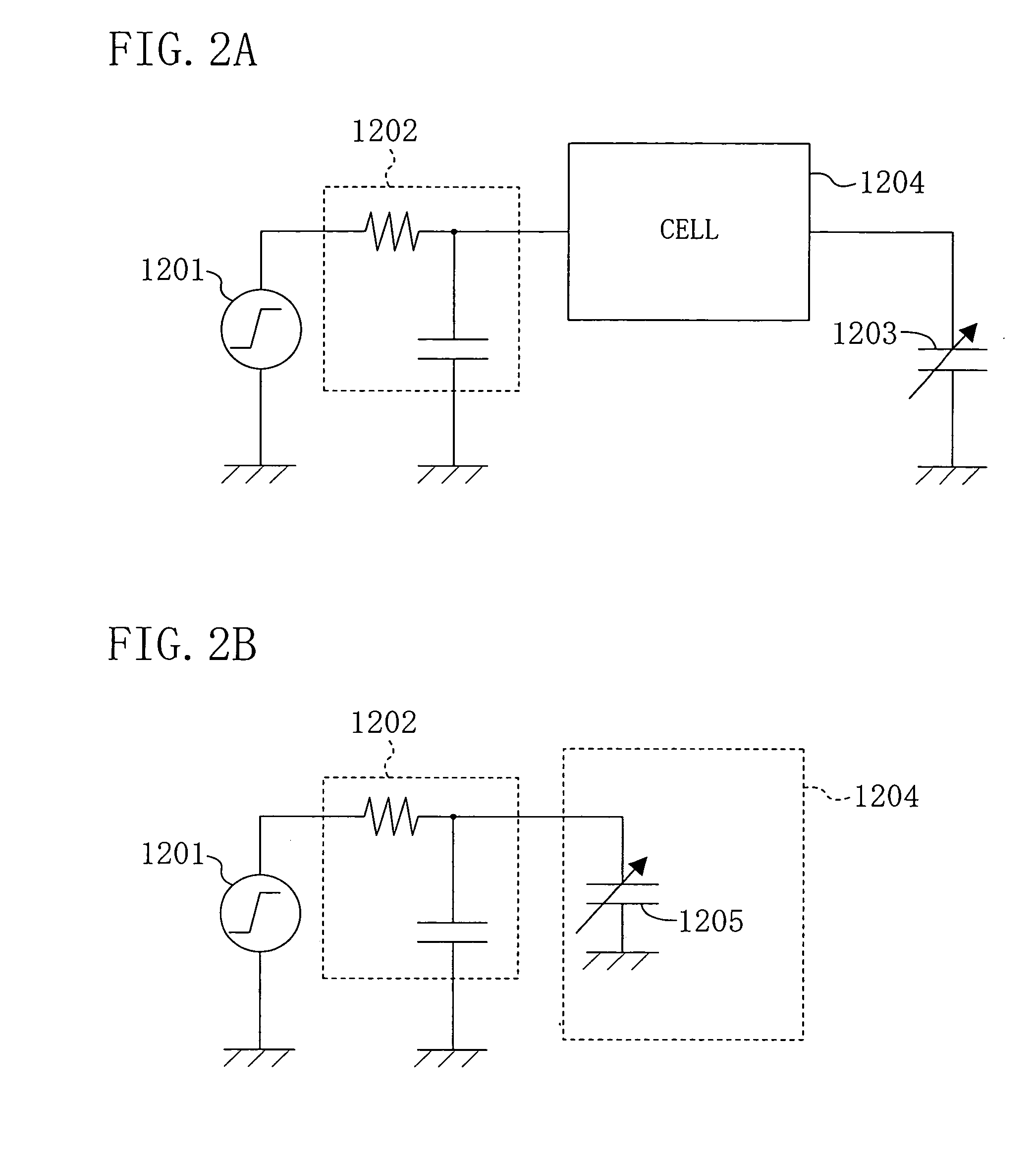
[0092]FIG. 7 is a circuit subjected to characterization for the purpose of verifying waveform distortion in a delay time calculation method in which waveform distortion is considered. In FIG. 7, the input terminal side of a characterization subject cell (delay time calculation subject circuit) C1 is connected to a cell C2 which has a small driving capacity. The output terminal side of the characterization subject cell C1 is connected to a load capacitor C3 which is driven by the characterization subject cell C1. The voltage input to the cell C2 of a small driving capacity has a waveform C4. The voltage input to the characterization subject cell C1 has a waveform C5. The voltage output from the characterization subject cell C1 has a waveform C6. In the circuit of FIG. 7, the cell C2 of a small driving capacity is connected to the input side of the characterization subject cell C1, and theref...


PUM


Abstract

An effective input terminal capacitance which is effectively equivalent to a cell in which a waveform distortion is caused due to the Miller effect and a drive load connected to the cell is calculated in advance, and the cell and the drive load are replaced by the calculated effective input terminal capacitance, while considering that the Miller effect is caused according to the size of the drive load driven by a delay time calculation subject circuit, such as a cell, or the like, and a distortion occurs in input and output waveforms of the delay time calculation subject circuit due to the Miller effect. Thereafter, a circuit simulation is carried out using the effective input terminal capacitance. A resultant effective input terminal capacitance value is characterized as a function of an input slope waveform and the drive load and converted to table data.

Description

CROSS-REFERENCES TO RELATED APPLICATION [0001] This Non-provisional application claims priority under 35 U.S.C. §119(a) on Patent Application No. 2004-123450 filed in Japan on Apr. 19, 2004, the entire contents of which are hereby incorporated by reference. BACKGROUND OF THE INVENTION [0002] The present invention relates to a method for characterizing the characteristics of cells subjected to a delay time calculation with consideration for a waveform distortion in a semiconductor integrated circuit, which is provided for the purpose of performing a circuit design with consideration for a waveform distortion. The present invention further relates to a delay time calculation method using the characterization method. [0003] In a general cell characteristic characterization method used in the preparation of a library for gate-level delay time calculation, various values of the input transition value and drive load are assigned to a cell subjected to a characterization (characterization ...

Claims


Application Information

Patent Timeline
Patent Type & Authority Applications(United States)
IPC IPC(8): G06F17/50G11C8/00
CPCG06F17/5036G06F30/367
Inventor ISHIBASHI, NORIKOAMEKAWA, NAOKIIWANISHI, NOBUFUSA
Owner PANASONIC CORP
Why Eureka
Try Eureka