Field emission device (FED)

Inactive Publication Date: 2005-10-27
SAMSUNG SDI CO LTD
View PDF10 Cites 6 Cited by
  • Summary
  • Abstract
  • Description
  • Claims
  • Application Information

AI Technical Summary

Benefits of technology

[0009] The present invention provides an FED that efficiently protects

Problems solved by technology

Accordingly, when emitting electrons, an electrochemical potential is increased at the emission ends of the CNTs, resulting in the degradation of the emission ends of the CNT

Method used


Image

  • Field emission device (FED)
  • Field emission device (FED)
  • Field emission device (FED)

Examples


first embodiment

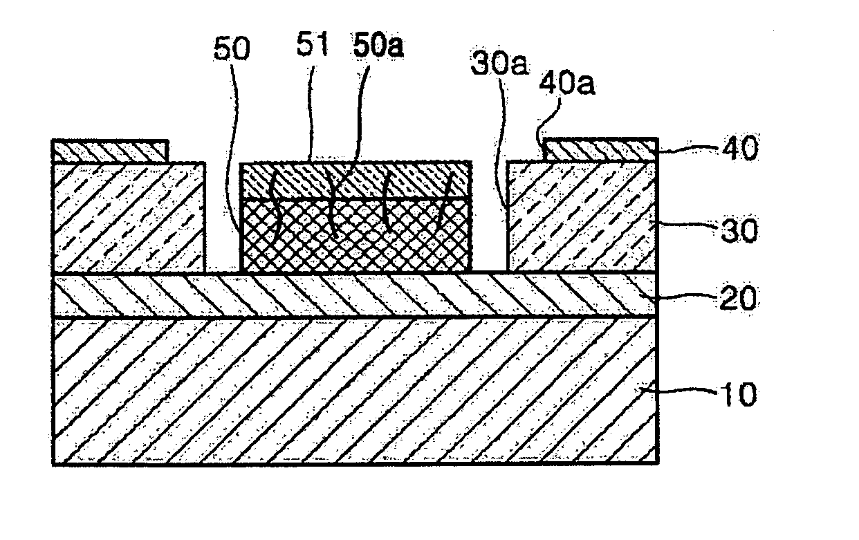
[0044] First Embodiment

[0045] Referring to FIG. 2, a cathode electrode 20 is formed on a substrate 10, and a gate insulating layer 30 is formed on the cathode electrode 20. A through hole 30a to receive a CNT emitter 50 is formed in the gate insulating layer 30, and the CNT emitter 50 to emit electrons is formed at the bottom of the through hole 30a. The CNT emitter 50 is formed on a portion of the cathode electrode 20 that is exposed through the bottom of the through hole 30a. The CNT emitter 50 includes a plurality of CNTs 50a and can further include a conductive material, for example, Ag particles, for efficiently supplying currents to the CNTs 50a.

[0046] A stabilizer layer 51 to stabilize the emission from the CNTs while protecting the CNTs is coated on the CNT emitter 50. The stabilizer layer 51 permits the emission of electrons from the CNTs 50a and covers the CNTs 50a on the surface of the CNT emitter 50. An example of the stabilizer layer 51 includes any one material or a m...

second embodiment

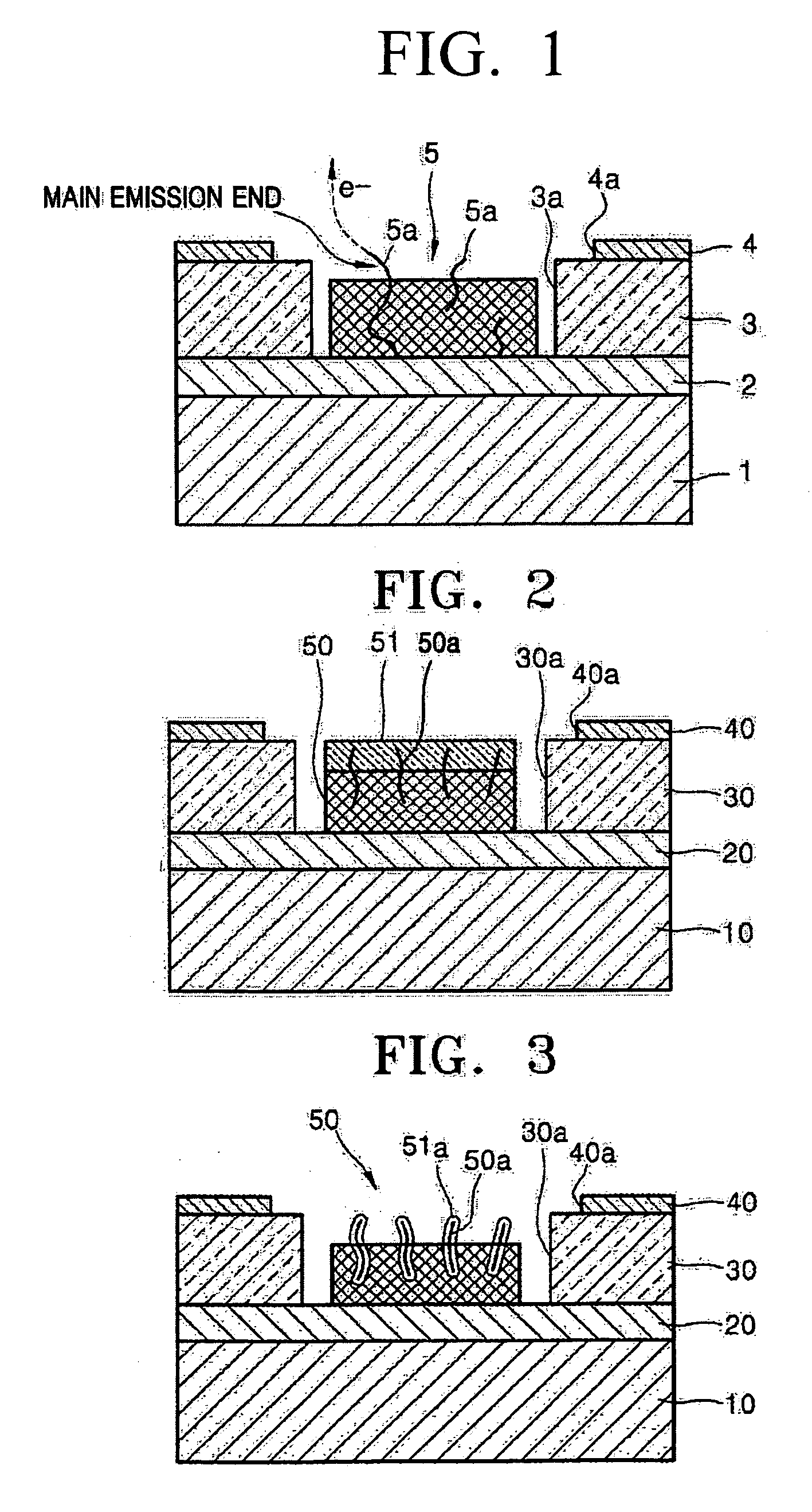
[0049] Second Embodiment

[0050] Referring to FIG. 3, a cathode electrode 20 is formed on a substrate 10, and a gate insulating layer 30 is formed on the cathode electrode 20. A through hole 30a to receive a CNT emitter 50 is formed in the gate insulating layer 30, and the CNT emitter 50 to emit electrons is formed at the bottom of the through hole 30a. The CNT emitter 50 is formed on a portion of the cathode electrode 20 that is exposed through the bottom of the through hole 30a. The CNT emitter 50 includes a plurality of CNTs 50a and can further include a conductive material, for example, Ag particles, for efficiently supplying currents to the CNTs 50a.

[0051] Stabilizer layers 51a for stabilizing the emission from the CNTs 50a are coated on the surfaces of the CNTs 50a. Examples of the stabilizer layers 51 a include SiO2, MgO, TiO2, BN, RuOx, and PdOx. In addition, the stabilizer layer 51a is formed to a thickness of 1 to 100 nm in order to permit the emission of electrons.

[0052] ...

third embodiment

[0078] Third Embodiment

[0079] Referring to 9, a cathode electrode 20 is formed on a substrate 10, and a gate insulating layer 30 is formed on the cathode electrode 20. A through hole 30a to receive a CNT emitter 50 is formed in the gate insulating layer 30, and the CNT emitter 50 to emit electrons is formed at the bottom of the through hole 30a. The CNT emitter 50 is formed on a portion of the cathode electrode 20 that is exposed through the bottom of the through hole 30a. The CNT emitter 50 includes a plurality of CNTs 50b that are grown on the cathode electrode 20.

[0080] Stabilizer layers 51b for stabilizing the emission from the CNTs 50b are coated on the upper ends of the CNTs 50b, which are perpendicularly grown on the cathode electrode 20, in other words, the emission ends of the CNTs 50b. An example of the stabilizer layer 51b includes any one material or a mixture of at least two materials selected from a group formed of SiO2, MgO, TiO2, BN, RuOx, and PdOx. In addition, the...


PUM


Abstract

A Field Emission Device (FED) includes an emitter formed on a cathode electrode and including Carbon NanoTubes (CNTs), and a gate electrode to extract electrons from the emitter. In addition, a RuOx layer or a PdOx layer is coated on the emitter to protect the CNTs and to stabilize the emission from the CNTs. A stabilizer layer to stabilize an emission structure and to protect emission ends is coated on the surface of a CNT emitter or the surfaces of the CNTs, more specifically, the emission ends of the CNTs, in order to prevent abrasion of the CNTs caused by an excess current or an emission process.

Description

CLAIM OF PRIORITY [0001] This application makes reference to, incorporates the same herein, and claims all benefits accruing under 35 U.S.C. § 119 from an application entitled FIELD EMISSION DEVICE filed with the Korean Intellectual Property Office on Apr. 27, 2004, and there duly assigned Serial No. 10-2004-0029194. BACKGROUND OF THE INVENTION [0002] 1. Field of the Invention [0003] The present invention relates to an Field Emission Device (FED), and more particularly, to an FED with improved emission stability and durability. [0004] 2. Description of the Related Art [0005] A carbon NanoTube (CNT) generates field emission even at a low voltage due to a small diameter and a sharp end. U.S. Pat. No. 6,339,281 relates to a Field Emission Array (FEA) using an emitter mixed paste and a method of manufacturing the FEA. U.S. Pat. No. 6,440,761 relates to an FEA using CNTs, which are formed by a growing method, as an emitter, and a method of manufacturing the FEA. In general, it is conveni...

Claims


Application Information

Patent Timeline
IPC IPC(8): H01J1/304H01J1/02H01J1/30H01J3/02
CPCB82Y10/00H01J2201/30469H01J3/022H01J1/3042H01J1/30
Inventor LEE, JEONG-HEEJEONG, TAE-WONKIM, WON-SEOKLEE, SANG-HYUNLEE, HYUN-JUNGHUH, JEONG-NA
Owner SAMSUNG SDI CO LTD
Why Eureka
Try Eureka