

Substrate manufacturing method
a manufacturing method and technology of substrates, applied in the direction of semiconductor substrates, basic electric elements, electrical equipment, etc., can solve the problems of difficult to reduce metal contamination, difficult to manufacture semiconductor substrates at a low cost, and metal contamination from atmospheric gas or the components of the annealing furnace in use, so as to reduce metal contamination
- Summary
- Abstract
- Description
- Claims
- Application Information
AI Technical Summary
Benefits of technology
Problems solved by technology
Method used
Image

Examples
first embodiment
[First Embodiment]
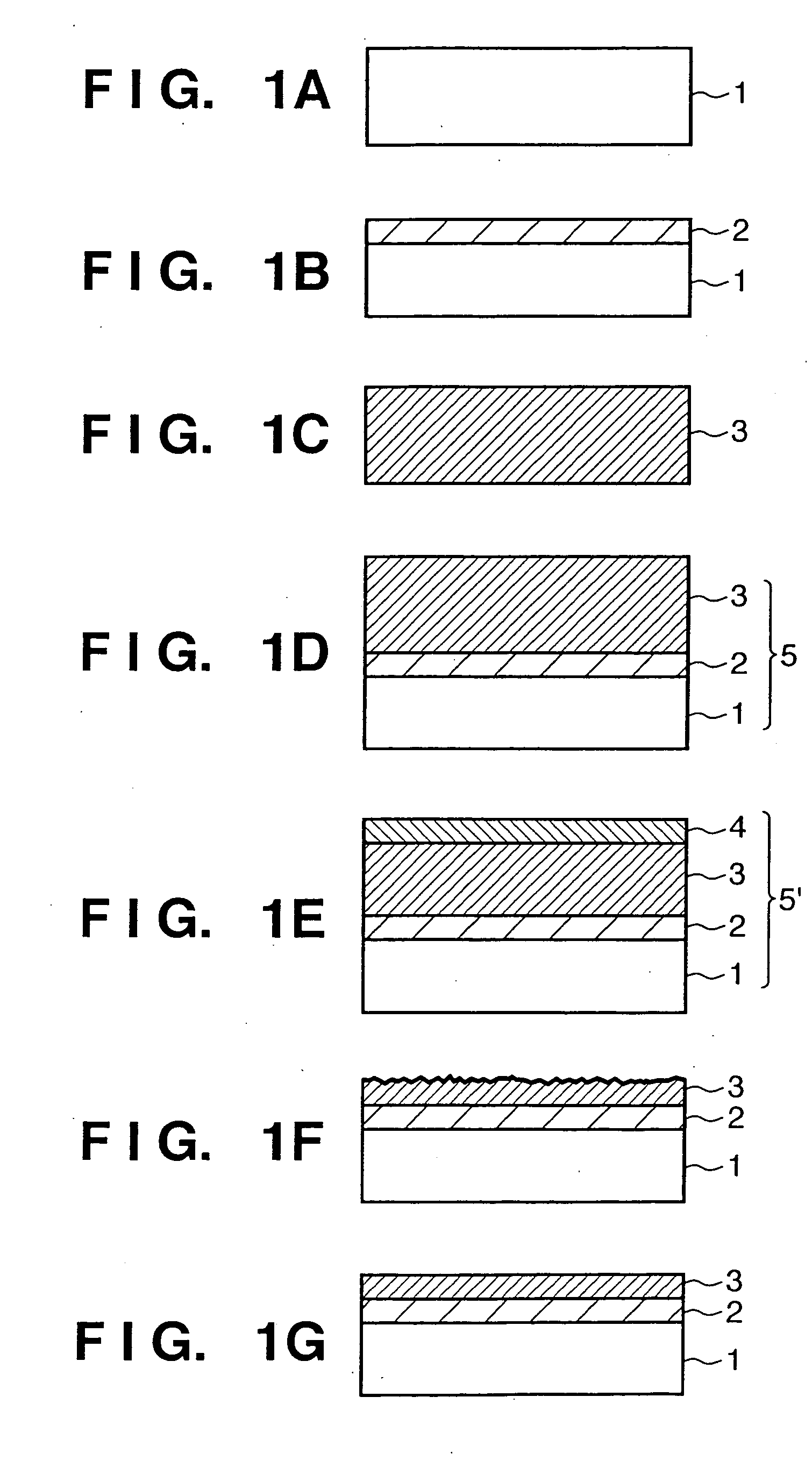
[0023]FIGS. 1A to 1G are views showing a substrate manufacturing method according to the first embodiment of the present invention.
[0024] As the substrate manufacturing method according to the first embodiment of the present invention, a method of manufacturing a substrate such as a SOI substrate will be described as an example. FIGS. 1A to 1G are views for explaining the substrate manufacturing method according to the preferred embodiment of the present invention.
[0025] In the step shown in FIG. 1A, a first semiconductor substrate (support substrate) 1 is prepared. As the first semiconductor substrate 1, a substrate containing Si, Ge, SiGe, SiC, C, GaAs, GaN, AlGaAs, InGaAs, InP, or InAsSi, a substrate obtained by forming an insulator on these substrates, a transparent substrate such as a quartz substrate, or a sapphire substrate can be used.
[0026] In the step shown in FIG. 1B, an insulating layer 2 is formed on the first semiconductor substrate (support substr...
second embodiment
[Second Embodiment]
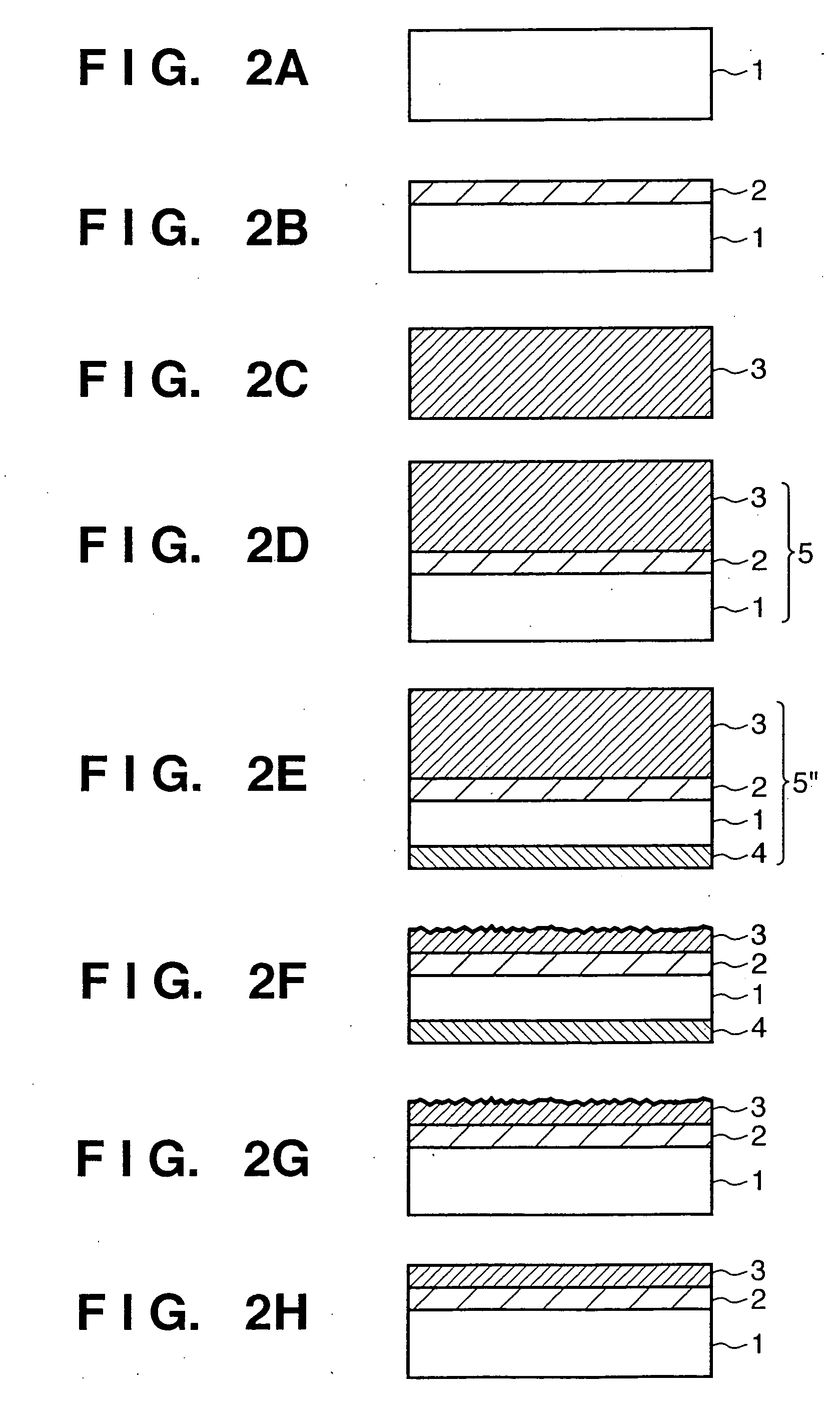
[0034]FIGS. 2A to 2H are views showing a substrate manufacturing method according to the second embodiment of the present invention.
[0035] As the substrate manufacturing method according to the second embodiment of the present invention, a method of manufacturing a substrate such as a SOI substrate will be described as an example. FIGS. 2A to 2H are views for explaining the substrate manufacturing method according to the preferred embodiment of the present invention. The same reference numerals as in FIGS. 1A to 1G denote the same or similar elements in FIGS. 2A to 2H.
[0036] The steps shown in FIGS. 2A to 2D are substantially the same as those shown in FIGS. 1A to 1D in the substrate manufacturing method according to the first embodiment.
[0037] In the step shown in FIG. 2E, a gettering layer 4 having a gettering site to capture an internal metal contamination is formed on the exposed surface on the side of a first semiconductor substrate 1 serving as a support ...
third embodiment
[Third Embodiment]
[0043]FIGS. 3A to 3H are views showing a substrate manufacturing method according to the third embodiment of the present invention.
[0044] As the substrate manufacturing method according to the third embodiment of the present invention, a method of manufacturing a substrate such as a SOI substrate will be described as an example. FIGS. 3A to 3H are views for explaining the substrate manufacturing method according to the preferred embodiment of the present invention. The same reference numerals as in FIGS. 1A to 1G and 2A to 2H denote the same or similar elements in FIGS. 3A to 3H.
[0045] The steps shown inFIGS. 3A to 3D are substantially the same as those shown in FIGS. 1A to 1D in the substrate manufacturing method according to the first embodiment.
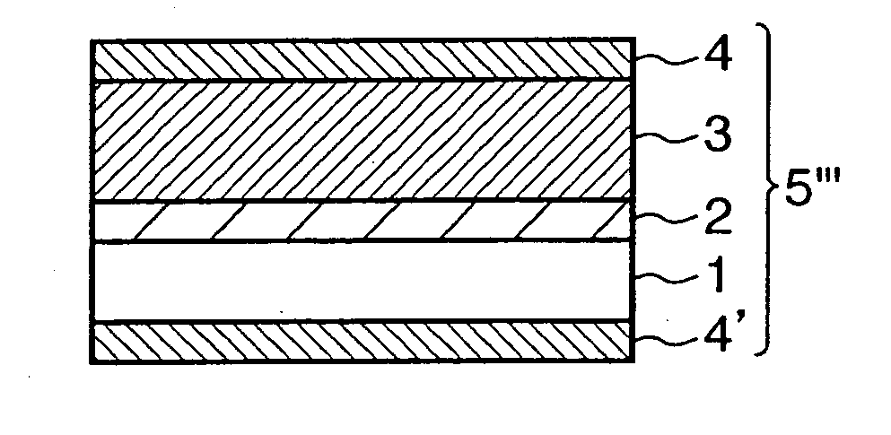
[0046] In the step shown in FIG. 3E, gettering layers 4 and 4′ each having a gettering site to capture an internal metal contamination are formed on the surface on the side of a second semiconductor substrate 3 serving...
PUM
 Abstract
Description
Claims
Application Information