High-frequency switch circuit and high-frequency transmitting/receiving apparatus

a switch circuit and high-frequency technology, applied in the field of high-frequency switch circuits, can solve the problems of limited resistance and off-capacitance, limited isolation, and loss of spdt, and achieve the effect of greater off-capacitance for the width of the unit ga

Inactive Publication Date: 2005-10-27
KK TOSHIBA
View PDF5 Cites 82 Cited by
  • Summary
  • Abstract
  • Description
  • Claims
  • Application Information

AI Technical Summary

Problems solved by technology

In effect, however, the on resistance and the off-capacitance are limited.
Inevitably, the SPDT has an insertion loss even if it assumes the through state, and has a limited isolation even if it assumes the off state.
These parasitic inductances result from the leads and bonding wires of the package containing the circuit.
They adversely influence the characteristics of the SPDT switch.
As can be understood from the above, the conventional SPDT switch has a large transmission loss due to the parasitic inductance of the leads and bonding wires of the package.
This increases the area of the output-matching circuit and, ultimately, the manufacturing cost thereof.

Method used


Image

  • High-frequency switch circuit and high-frequency transmitting/receiving apparatus
  • High-frequency switch circuit and high-frequency transmitting/receiving apparatus
  • High-frequency switch circuit and high-frequency transmitting/receiving apparatus

Examples


first embodiment

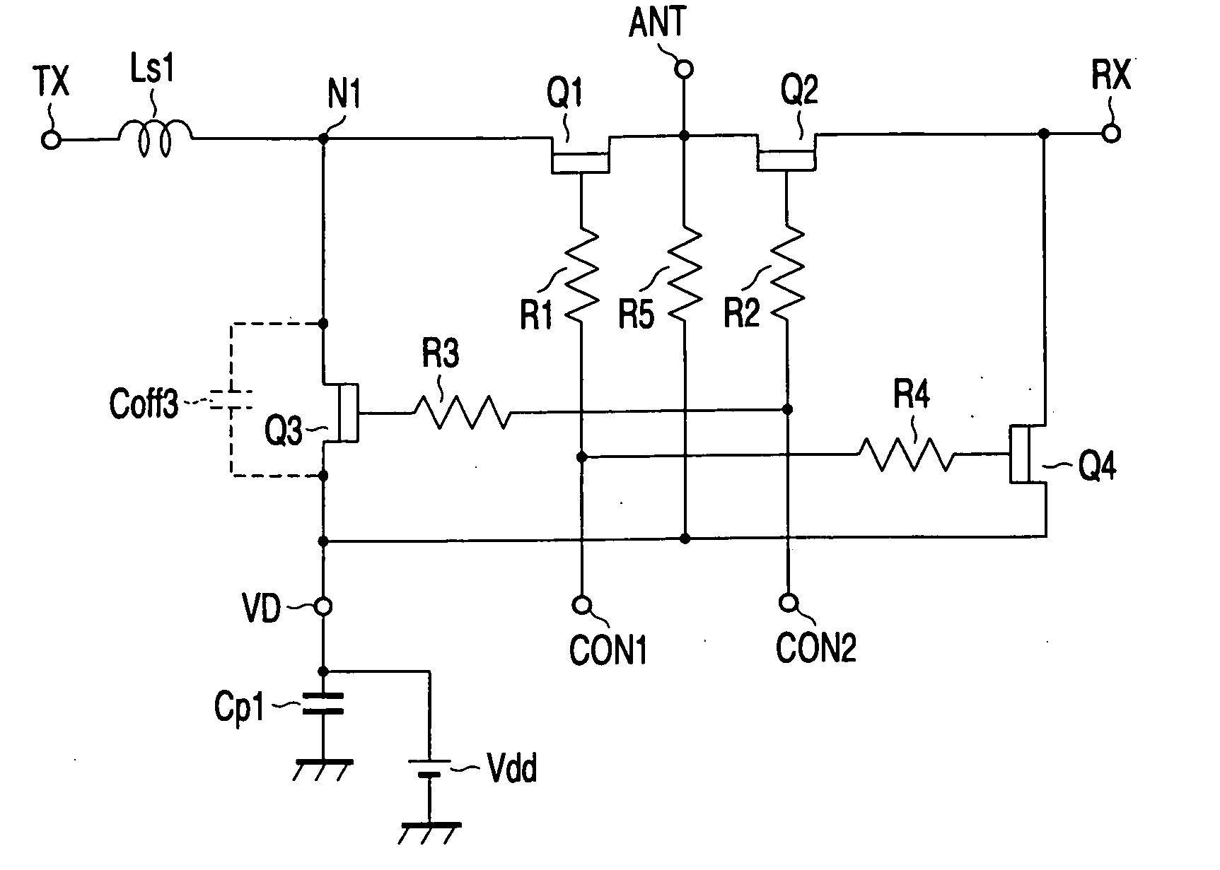
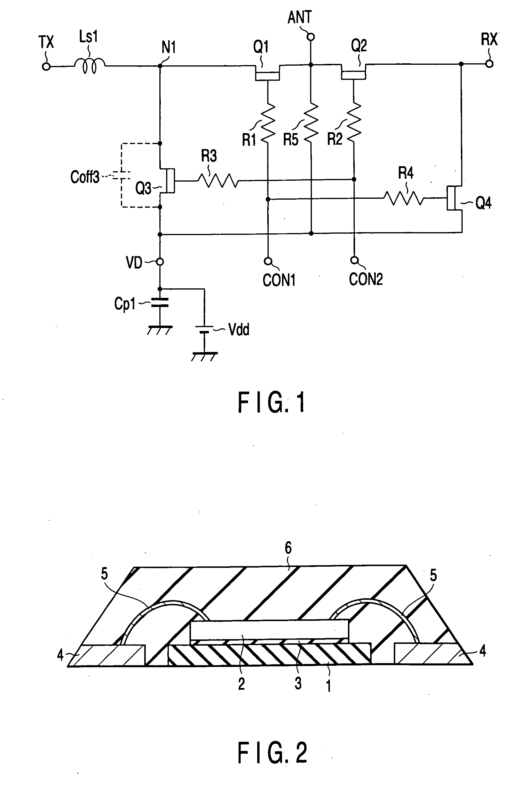
[0041]FIG. 1 is a circuit diagram that shows an SPDT switch according to the first embodiment of the invention. The SPDT switch has an antenna terminal ANT, a transmission terminal TX, a receipt terminal RX, two control terminals CON1 and CON2, and a power-supply voltage terminal VD.

[0042] The antenna terminal ANT is connected to an antenna. The transmission terminal TX is connected to the output of a high-frequency power amplifier (not shown) that is configured to amplify, for example, a signal to be transmitted. The signal to be transmitted is supplied to the transmission terminal TX. The receipt terminal RX is connected to the input of a receiving-side low noise amplifier (not shown). This terminal RX receives a signal from the antenna terminal ANT.

[0043] The power-supply voltage Vdd is applied to the power-supply voltage terminal VD. The terminal VD is connected to a decoupling capacitor Cp1, which is connected to the ground. In other words, the terminal VD is grounded for a h...

second embodiment

[0078] The second embodiment of the invention is an SPDT switch, too. This SPDT switch has metal wires that differ in shape from those used in the first embodiment. The shunt FET Q3 therefore has a larger off-capacitance than its counterpart of the first embodiment.

[0079]FIG. 5 is a sectional view depicting the structure of the transmitting-side shunt FET Q3 incorporated in the SPDT switch according to the second embodiment. A metal wire 15 has an overhang 15a that overlaps the gate electrode 11. An inter-layer insulating layer 17 fills the gap between the gate electrode 11 and the overhang 15a. A metal wire 16 has an overhang 16a that overlaps the gate electrode 11. The inter-layer insulating layer 17 fills the gap between the gate electrode 11 and the overhang 16a. Note that the gate electrode 11 has two overhangs 11a and 11b as in the first embodiment.

[0080]FIG. 6 is an equivalent-circuit diagram of the off-capacitance at the shunt FET Q3 shown in FIG. 5. Capacitance C34 is cap...

third embodiment

[0084] The third embodiment of the invention is also an SPDT switch. This SPDT switch has a shunt FET Q3 that is a multi-gate FET. Namely, the shunt FET Q3 has a plurality of gates and therefore exhibits a high withstand voltage to the input signal. Including a multi-gate FET, the SPDT switch has a high withstand voltage to high-frequency signals.

[0085]FIG. 7 is a sectional view depicting the structure of the transmitting-side shunt FET Q3 provided in the third embodiment. As seen from FIG. 7, the shunt FET Q3 is a triple-gate FET, i.e., an FET having three gate electrodes 11, 18 and 19.

[0086] The gate electrodes 18 and 19, each having a T-shaped cross section, are formed on the semiconductor substrate 10. Insulating films 20 are provided between the overhangs of the gate electrode 18 and the semiconductor substrate 10. Insulating films 20 are interposed between the overhangs of the gate electrode 19 and the semiconductor substrate 10. The insulating films 20 are made of, for exam...


PUM


Abstract

A high-frequency switch circuit includes a first terminal which receives a transmission signal, a first FET which makes a path of the transmission signal conductive or cut off, a second terminal which receives a control signal that is inactive in a transmitting mode and is active in a receiving mode, a ground terminal which is grounded via a first capacitor, and a second FET which has a drain electrode, a source electrode and a gate electrode, the drain or source electrode being connected to the ground terminal, the source or drain electrode being connected to first terminal, and the gate electrode being connected to the second terminal, and which has a greater off-capacitance for unit gate width than the first FET.

Description

CROSS-REFERENCE TO RELATED APPLICATIONS [0001] This application is based upon and claims the benefit of priority from prior Japanese Patent Application No. 2004-131608, filed Apr. 27, 2004, the entire contents of which are incorporated herein by reference. BACKGROUND OF THE INVENTION [0002] 1. Field of the Invention [0003] The present invention relates to a high-frequency switch circuit that can switch a high-frequency signal-transmitting mode to a high-frequency signal-receiving mode, and vice versa. More particularly, the invention relates to an SPDT (Single-Pole Double-Throw) switch that handles high-frequency signals. [0004] 2. Description of the Related Art [0005] Generally, a SPDT switch is incorporated in high-frequency communications apparatuses such as mobile telephones. The SPDT switch includes a semiconductor switch for switching the signal transmission to the reception of signal and vice versa. The SPDT switch is a high-frequency switch that receives a signal from an inp...

Claims


Application Information

Patent Timeline
Patent Type & Authority Applications(United States)
IPC IPC(8): H03K17/00H01P3/00H01P9/00H03K17/693H04B1/38H04B1/44H04B1/48
CPCH04B1/48
Inventor SAGAE, YOSHITOMOSESHITA, TOSHIKI
Owner KK TOSHIBA
Why Eureka
Try Eureka