

Gate-level netlist reduction for simulating target modules of a design
a target module and gate-level technology, applied in the field of circuit design simulation, can solve the problems of significant hardware resources consumed by the simulator of electronic design automation (eda), and the simulation of an entire asic design imposes a significant burden in terms of cpu time and hardware resources, so as to improve the turnaround time of design validation, reduce the time spent, and reduce the effect of iterations
- Summary
- Abstract
- Description
- Claims
- Application Information
AI Technical Summary
Benefits of technology
Problems solved by technology
Method used
Image

Examples
Embodiment Construction
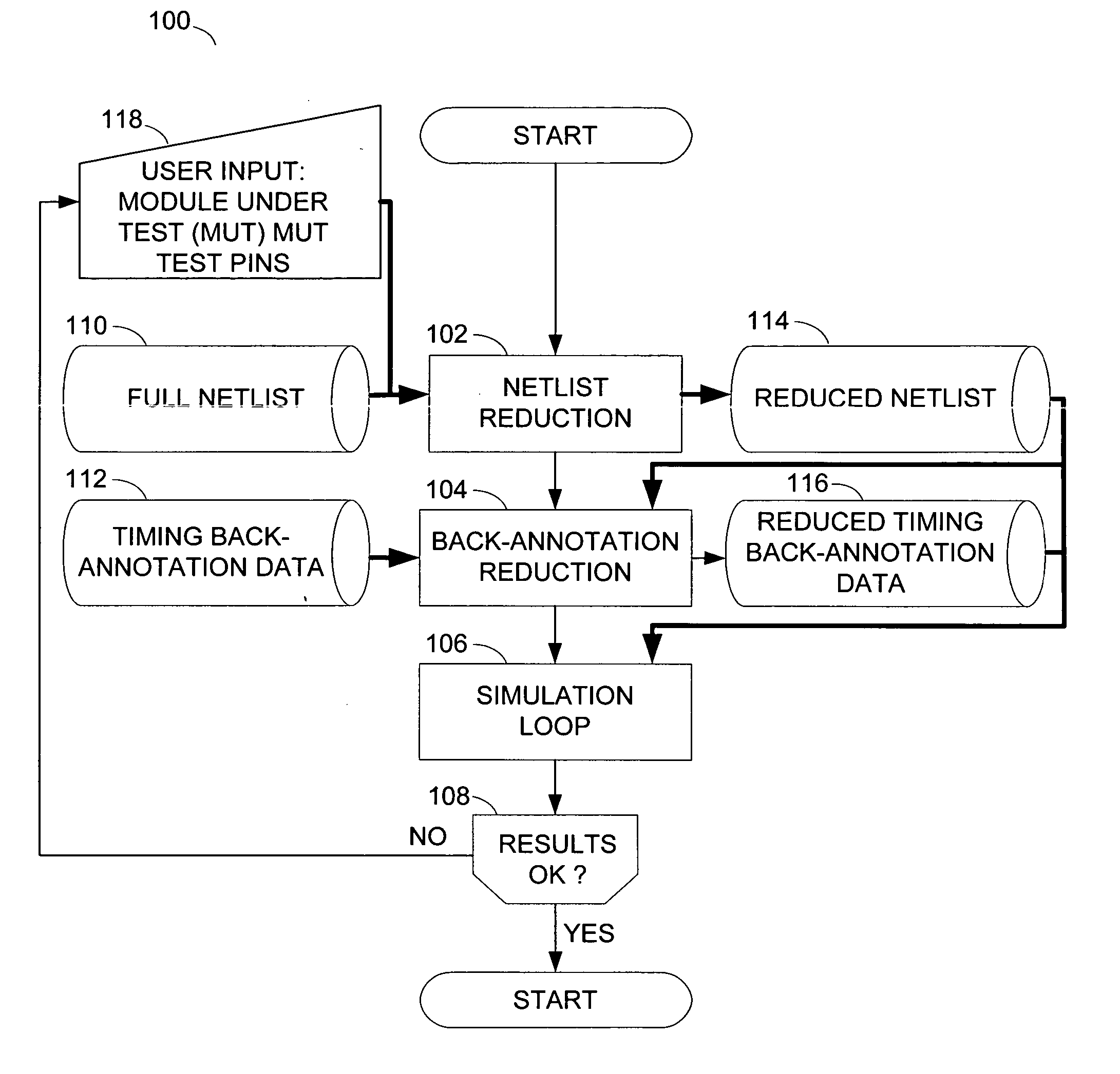
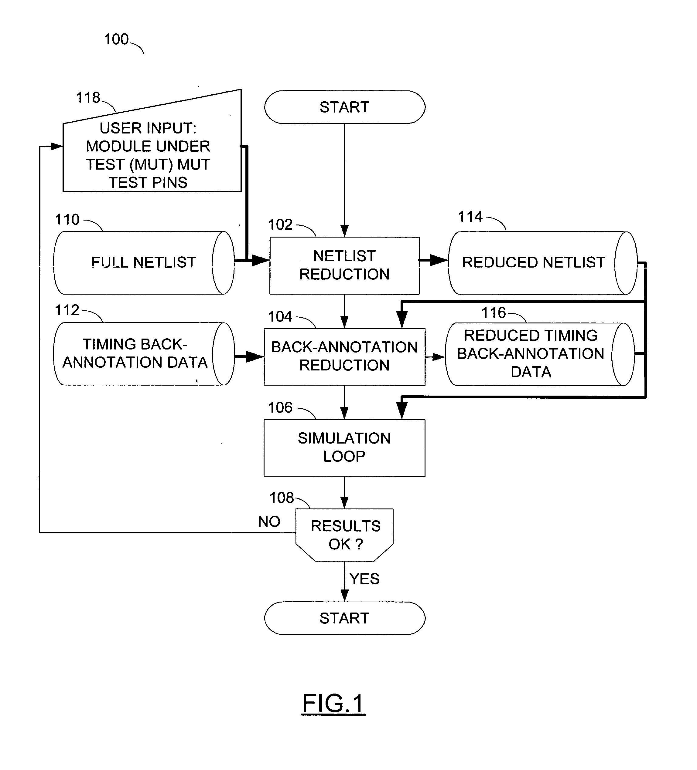
[0012] The present invention generally provides a novel method to improve design validation turnaround time by reducing gate-level simulation time. The gate-level simulation time reductions may be achieved by performing a selective reduction of a gate-level netlist for a circuit design. The method may identify all modules of the circuit design not involved in a simulation of a target module and may remove the unnecessary modules from the netlist. Back-annotation (e.g., timing) data may be adjusted accordingly to account for the reduced netlist. A simulator may then process a smaller netlist database than the full netlist for the circuit design.
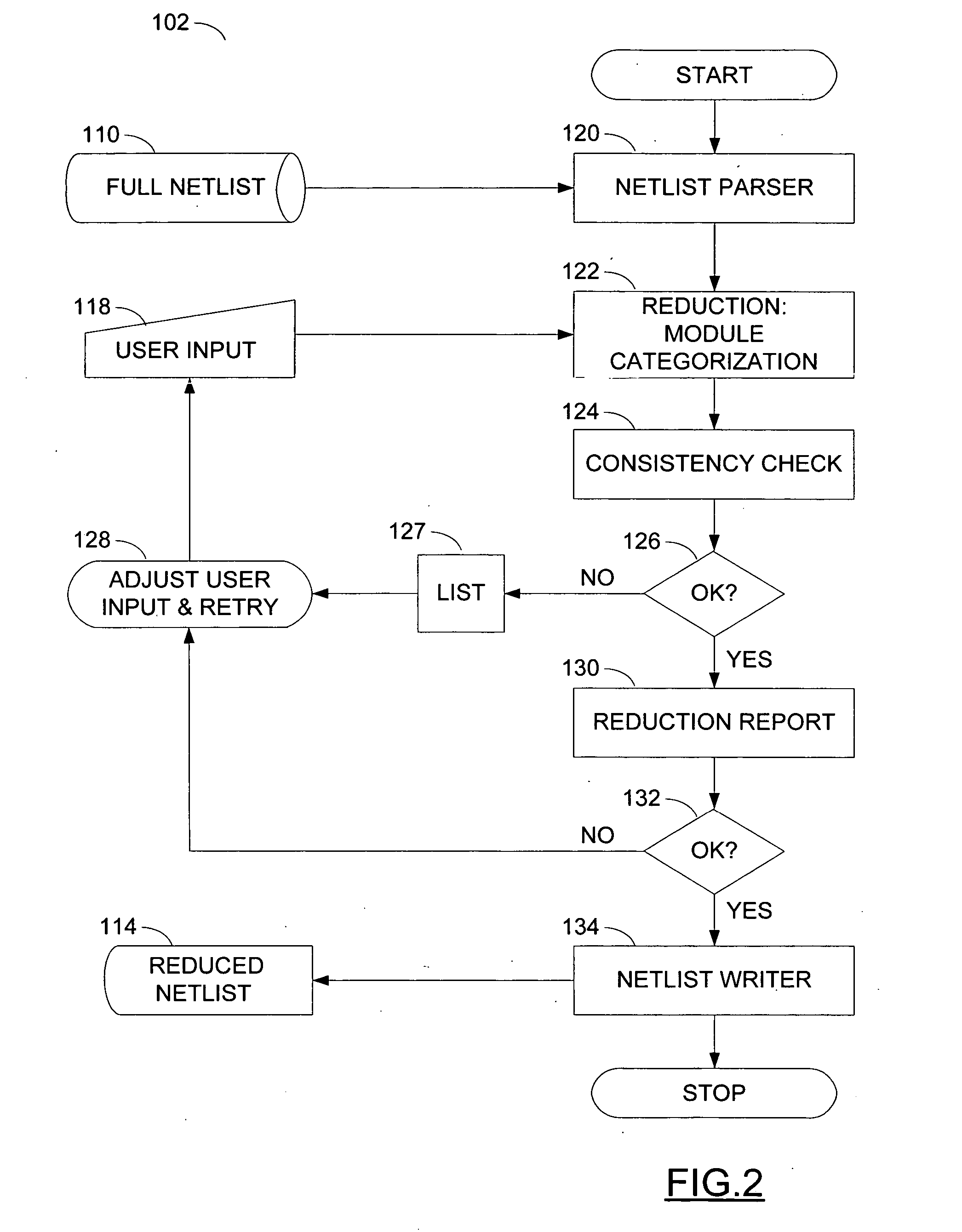
[0013] Referring to FIG. 1, a flow diagram of an example method 100 is shown in accordance with a preferred embodiment of the present invention. The method 100 may be referred to as a reduction method or process. The reduction method 100 generally comprises a step 102, a step 104, a step 106 and a step 108. The reduction method 100 generally ...
PUM
 Abstract
Description
Claims
Application Information