Differential/single-ended input stage

a single-ended input and input stage technology, applied in differential amplifiers, amplifiers with semiconductor devices/discharge tubes, amplifier details, etc., can solve the problems of low output power, low output power, and inability to provide an ideally flat passband, and achieve constant gain

Active Publication Date: 2005-11-03
SILICON LAB INC
View PDF17 Cites 12 Cited by
  • Summary
  • Abstract
  • Description
  • Claims
  • Application Information

AI Technical Summary

Problems solved by technology

Unfortunately, converting a single-ended signal from the antenna into a differential signal for the IC requires a balanced-to-unbalanced converter (balun).
Baluns tend to be expensive, introduce loss, and do not provide an ideally flat passband.
It is difficult to handle both single-ended and differential inputs, in large part due to the disparate input impedance requirements for the single-ended and differential inputs.

Method used


Image

  • Differential/single-ended input stage
  • Differential/single-ended input stage
  • Differential/single-ended input stage

Examples


Embodiment Construction

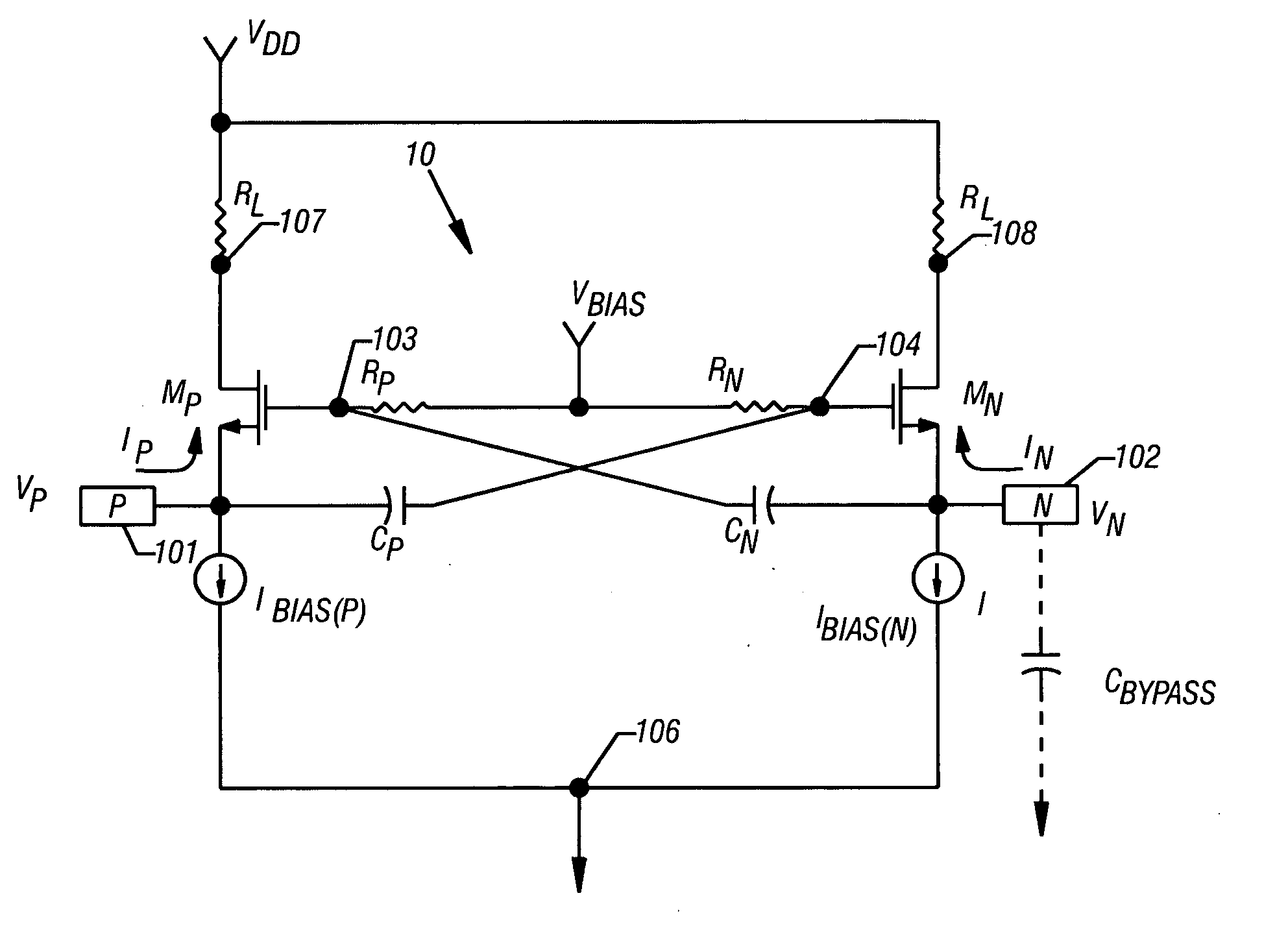
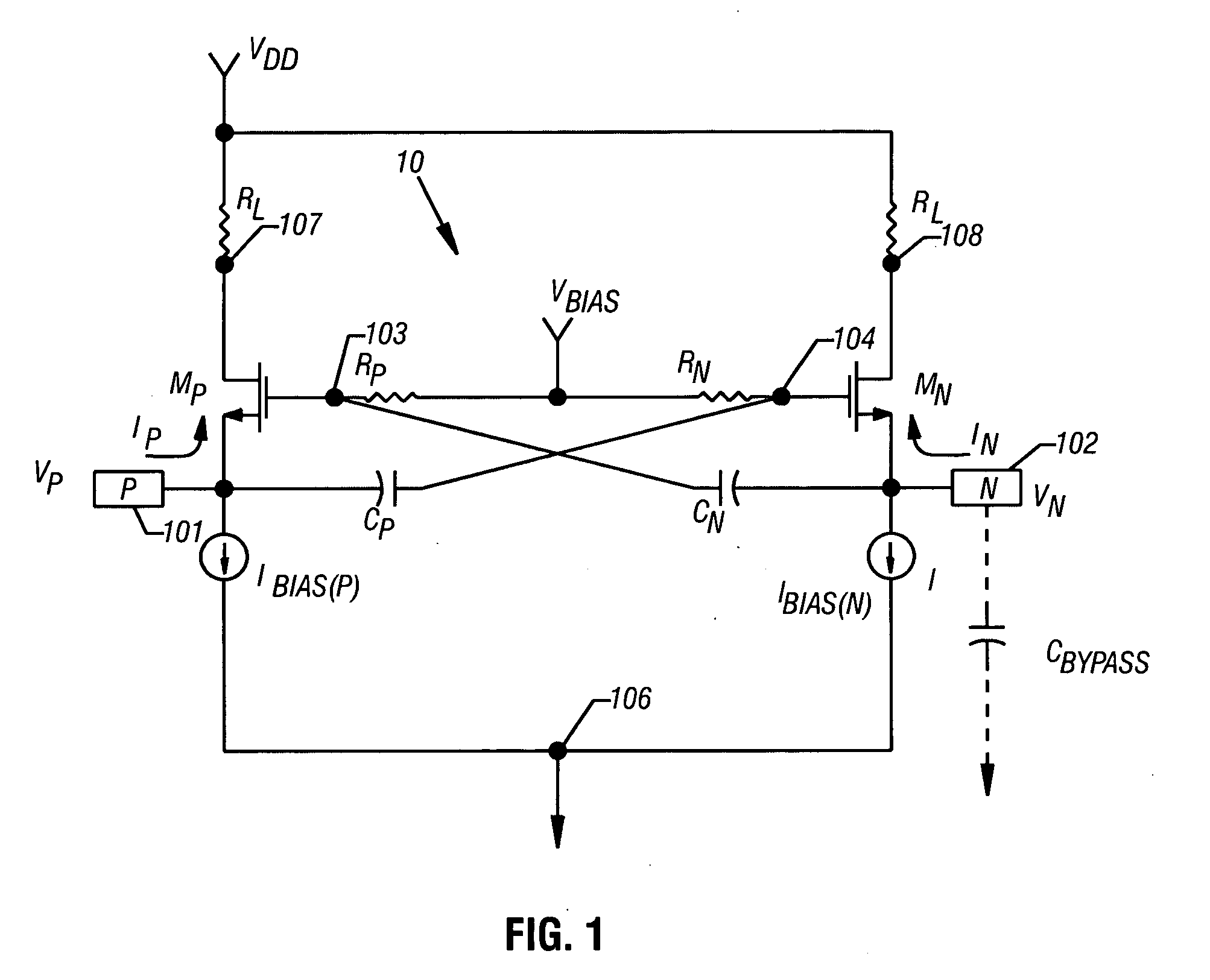
[0019] For an understanding of the subject differential / single-ended input stage, reference may be had to the following Detailed Description, including the appended claims, in connection with the above-described Drawings.

[0020] The invention instantiates a technique to selectably control the input stage of an IC device for either single-ended or differential operation. That is, the device is operable to accept either a differential or single-ended input signal and provide a differential output signal to a succeeding stage. In one embodiment, selection is effected by the connection of a capacitor to an input terminal. Further, the input stage is designed so that the gain of the input stage remains constant with respect to single-ended or differential operation. Accordingly, embodiments are applicable to all forms of circuitry that suggest a need to convert, or accept, either single-ended or differential signals. In single-ended operation, the circuit provides substantially the same ...


PUM


Abstract

An input stage for an integrated circuit device provides constant gain in selectable modes of either differential or single-ended operation. In one embodiment, transconductance devices are arranged so that the input impedance of the input stage matches the signal source impedance, regardless whether the input stage is selected to operate in a differential mode or in a single-ended mode. In accordance with an alternative embodiment, constant-gain and constant-impedance conditions are maintained in a configuration that comprises and input signal attenuator. In one application, the input stage may serve as a low-noise amplifier (LNA) for an integrated transceiver.

Description

FIELD OF THE INVENTION [0001] The invention relates generally to the design of integrated circuit devices and, more particularly, to an input stage that provides a more nearly optimal impedance match and constant gain, irrespective of whether a integrated circuit device is driven form a single-ended or from a differential input signal source. BACKGROUND [0002] Remarkable growth in the demand for communications products and services, and especially in the requirements for portable communications devices, has driven consumer requirements for low-cost, small-form-factor, low-power RF (radio frequency) transceivers. In addition, the development of state-of-the-art wireless applications has encouraged consumers to expect both the convenience of extended connectivity and the benefit of enhanced services. RF transceivers that operate in compliance with multiple prevailing standards are instrumental, if not required, in the satisfaction of these objectives. In this regard, the capabilities ...

Claims


Application Information

Patent Timeline
Patent Type & Authority Applications(United States)
IPC IPC(8): H03F3/45
CPCH03F3/45179H03F2200/372H03F2200/294
Inventor JOHNSON, RICHARD A.
Owner SILICON LAB INC
Why Eureka
Try Eureka