Low noise planar transformer

a transformer and low-noise technology, applied in the field of transformers, can solve the problems of increasing electromagnetic interference (emi), not readily adaptable to miniaturization or automated assembly, and high manufacturing cost of components, so as to reduce common mode noise, improve emi performance, and reduce common mode noise.

Active Publication Date: 2005-11-03
ASTEC INT LTD
View PDF6 Cites 35 Cited by
  • Summary
  • Abstract
  • Description
  • Claims
  • Application Information

AI Technical Summary

Benefits of technology

[0020] An advantage of the present invention is improved EMI performance by reducing common mode noise coupled from the primary winding to the secondary winding in a power transformer.
[0021] Another advantage of the present invention is that it reduces the common mode noise coupled to the secondary winding without increasing the leakage inductance.
[0022] Still another advantage of the present inventi

Problems solved by technology

The resulting components are expensive and time consuming to manufacture, and do not readily lend themselves to miniaturization or automated assembly.
One drawback of this arrangement is that it increases the capacitive coupling between the primary and secondary windings, which results in the generation of increased electromagnetic interference (EMI).
That is, due to the inter-winding capacitance of the transformer, common mode noise will be injected into the secondary.
This drawback is especially significant for a two switch forw

Method used


Image

  • Low noise planar transformer
  • Low noise planar transformer
  • Low noise planar transformer

Examples


Embodiment Construction

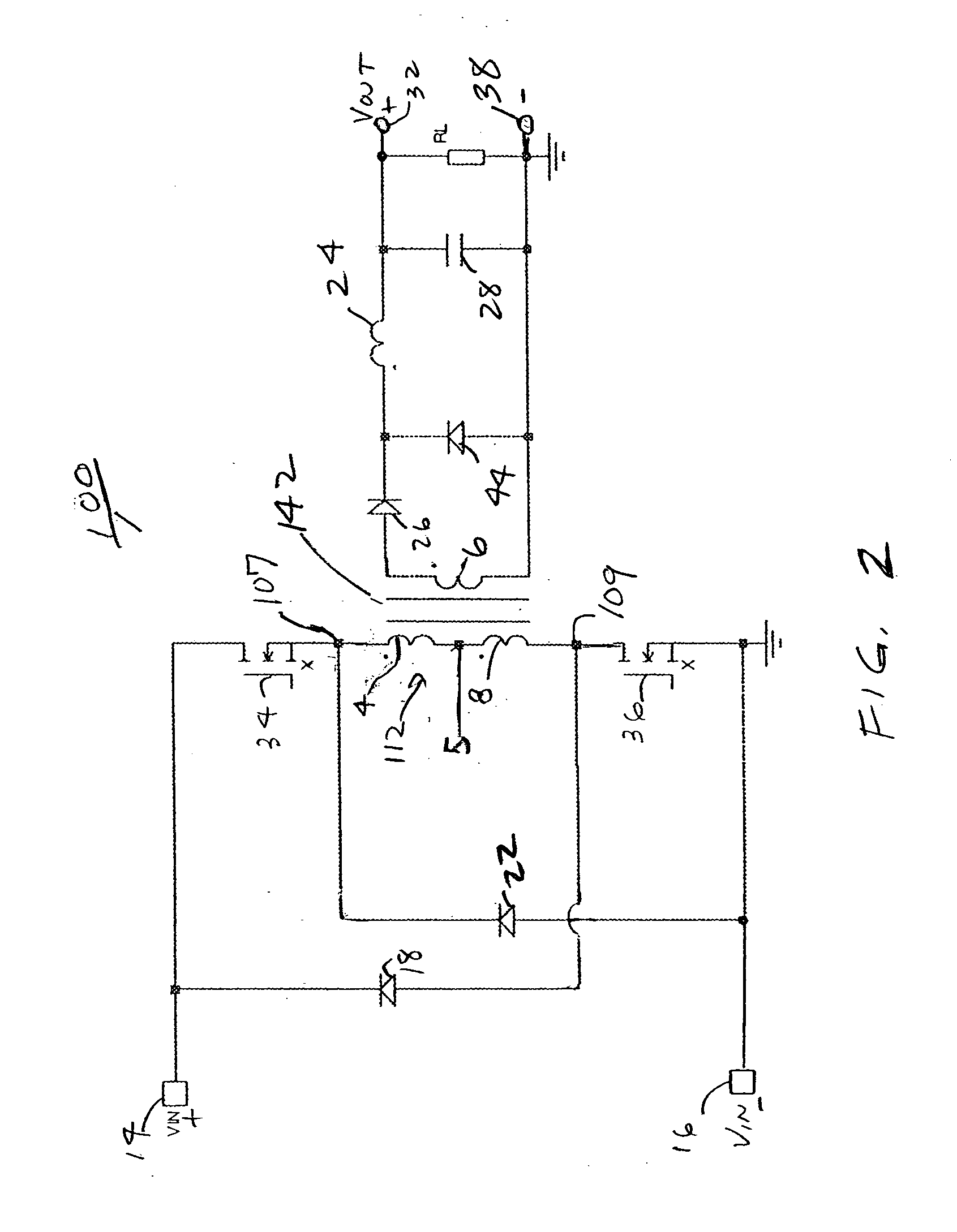
[0039]FIG. 2 shows a circuit diagram for a two switch forward converter 100 having an embodiment of the transformer according to the present invention. Converter 100 has an input terminal 14 to which an input DC voltage, Vin, is coupled, relative to a ground potential at an input terminal 16, and an output terminal 32 where the output DC voltage, VOUT, of the converter is provided relative to ground. Converter 100 includes a transformer 142 having a primary winding 112 and a secondary winding 6. Primary winding 112 comprises a first winding 4 and a second winding 8. Each winding has a first and second end. The second end of the first winding 4 is connected to the first end of second winding 8, at a node 5. A power switch 34 is coupled between the first end of first winding 4 at a node 107 and input terminal 14. A power switch 36 is connected to the second end of winding 8 at a node 109. The power switch 34 is connected in series with first winding 4, second winding 8, and power swit...


PUM


Abstract

An apparatus and method for reducing common mode noise capacitive coupling from a primary winding to a secondary winding in a transformer. In an embodiment, the primary winding has two terminals and a plurality of coil turns therebetween formed by a plurality of PCB layers sandwiched together, each having at least one of the coil turns formed thereon. The coils turns on each PCB layer are connected in a predetermined way to form the primary winding. Each terminal of the primary winding is connected to a coil turn on a separate corresponding PCB layer. The PCB layers are stacked layers to form the primary winding. The secondary winding or windings are positioned adjacent to a selected one of the stacked PCB layers that is in a position in the stack substantially midway between the first and second PCB layers. Preferably, the PCB layer closest to the secondary winding is comprised of only one coil turn so as to further minimize the common mode noise. In an alternative embodiment, the transformer windings are positioned in a secondary-primary-secondary arrangement wherein two halves of the primary winding are combined into one PCB winding. Alternatively, the present invention may be used for a planar matrix transformer.

Description

FIELD OF INVENTION [0001] The present invention relates to transformers, and more particularly a low noise planar transformer and a method of construction thereof. BACKGROUND OF THE INVENTION [0002] Electromagnetic components such as transformers have traditionally been constructed by winding one or more conductors about a cylindrical or toroidal core. This method of construction requires that a conductor, such as a wire, be wrapped around the outer surface of the core. The resulting components are expensive and time consuming to manufacture, and do not readily lend themselves to miniaturization or automated assembly. [0003] More recently, electromagnetic components have been constructed using printed circuit board (PCB) manufacturing techniques, where windings and individual winding turns are formed from a stack of PCB layers wherein each layer includes one or more conducting traces patterned on the surface of the PCB layer, or formed from a multi-layer PCB having such conducting t...

Claims


Application Information

Patent Timeline
IPC IPC(8): H01F5/00H01F17/00H01F27/28H01F27/34
CPCH01F17/0013H01F27/2804Y10T29/4902H01F2027/2819H01F27/34
Inventor SO, KELVIN WING CHI
Owner ASTEC INT LTD
Why Eureka
Try Eureka