
Input circuit for memory device

a technology of input circuit and memory device, which is applied in the field of input circuit of memory device, can solve problems such as data transmission speed slowness, and achieve the effect of improving data processing speed

Active Publication Date: 2005-11-03
SK HYNIX INC
View PDF4 Cites 2 Cited by
  • Summary
  • Abstract
  • Description
  • Claims
  • Application Information

AI Technical Summary

Benefits of technology

[0020] Accordingly, the present invention has been made to solve the above-mentioned problems occurring in the prior art, and it is an object of the present invention to provide an input circuit capable of improving a data processing speed by accelerating the operation time point of a data bus writer.

Problems solved by technology

In particular, a processing for input data is one of issues important for improving the data processing speed of the memory device.
Therefore, in the prior art, the operation time of the data bus writer is delayed by the time margin, so that a data transmission speed slows.

Method used


Image

  • Input circuit for memory device
  • Input circuit for memory device
  • Input circuit for memory device

Examples


Embodiment Construction

[0042] Hereinafter, a preferred embodiment of the present invention will be described with reference to the accompanying drawings.

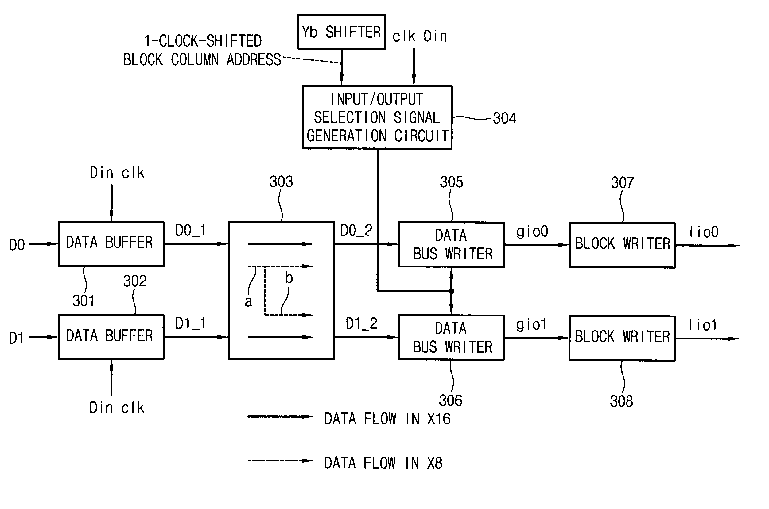
[0043]FIG. 3 is a block diagram showing a data input circuit according to the present invention. Hereinafter, a ×16 type in which the number of data buffers is 16 will be described.

[0044] The data input circuit of a memory device according to the present invention includes data buffers 301 and 302, an input multiplexer 303, a Yb shifter 309, an input selection signal generation circuit 304, data bus writers 305 and 306, and block writers 307 and 308. The data buffers 301 and 302 input data D0 and D1 applied from the external of the data input circuit, and the input multiplexer 303 is connected to the data buffers 301 and 302 and multiplexes the output data D0_1 and D1_1 of the data buffers 301 and 302. The Yb shifter 309 is a block column address shifter outputting a block column address one-clock delayed than a column address. The input selection signa...


PUM


Abstract

An input circuit for a semiconductor memory device is disclosed. The input circuit controlling transmission paths for data having passed through a data input buffer by using a 1-clock shifted block column address is provided. In particular, a data input apparatus improving a data processing speed by advancing an operation time point of a data bus writer is provided.

Description

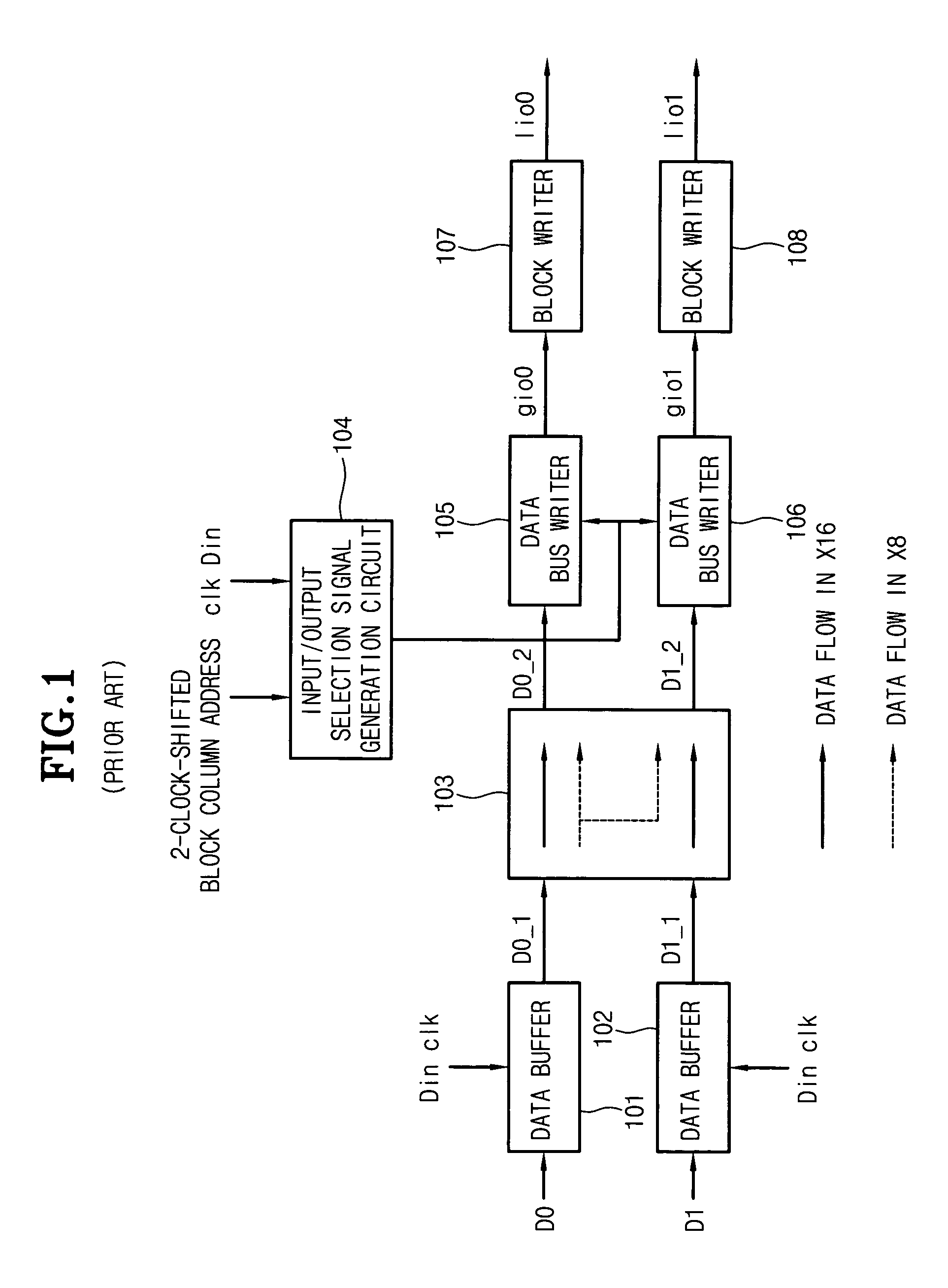
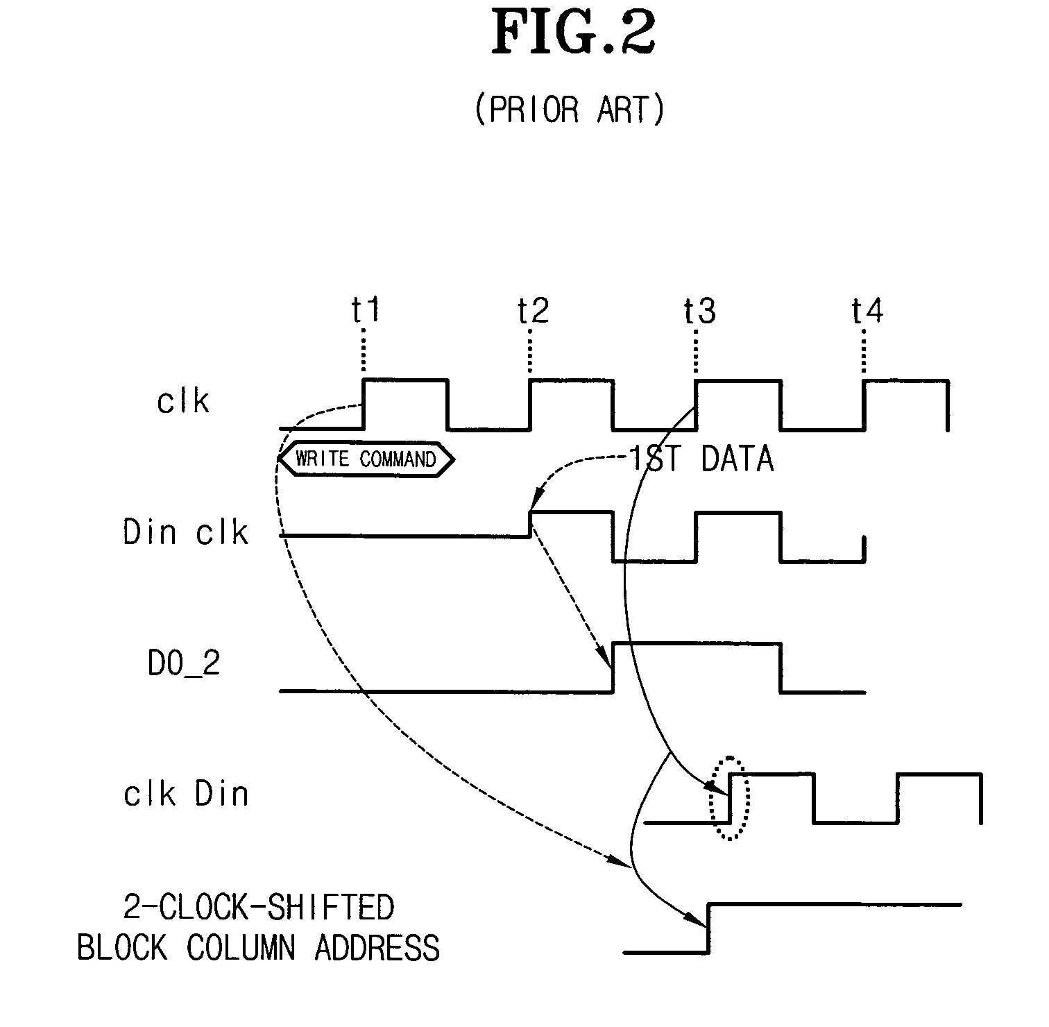
BACKGROUND OF THE INVENTION [0001] 1. Field of the Invention [0002] The present invention relates to an input circuit of a memory device, and more particularly to an input circuit for a memory device, which improves a data processing speed by controlling transmission paths for data having passed through a data input buffer in response to an input of a block address. [0003] 2. Description of the Prior Art [0004] The data processing speed of a semiconductor memory device is gradually accelerating. Moreover, with the development of a DDR SDRAM capable of accessing two data in one clock, the data processing speed of the memory device accelerates further. In particular, a processing for input data is one of issues important for improving the data processing speed of the memory device. [0005]FIG. 1 is a block diagram showing the data input circuit of a conventional memory device. Specifically, the memory device disclosed in the present specification denotes a DDR SDRAM, a DDR2 SDRAM (next...

Claims


Application Information

Patent Timeline
Patent Type & Authority Applications(United States)
IPC IPC(8): G11C5/00G11C11/4093G11C7/10
CPCG11C7/1078G11C7/1093G11C7/1087A61B18/203A61B18/22
Inventor LEE, CHANG HYUK
Owner SK HYNIX INC
Learn More