In-situ etch-stop etch and ashing in association with damascene processing in forming semiconductor interconnect structures

Inactive Publication Date: 2005-11-03
TEXAS INSTR INC
View PDF16 Cites 16 Cited by
  • Summary
  • Abstract
  • Description
  • Claims
  • Application Information

AI Technical Summary

Benefits of technology

[0011] One or more aspects of the present invention relate to forming single or dual damascene interconnect structures in the fabrication of semiconductor devices in manners that mitigate the above mentioned and other adverse effects. One or more aspects of the invention may be employed, for example, to facilitate better via critical dimension (CD) control, improve selectivity of etch-stop layer to inter layer dielectric (ILD) and / or intra-metal dielectric (IMD) material, and / or to simplify and make the flow of the fabrication process more efficient and / or cost effective.

Problems solved by technology

However, difficulties have been encountered in patterning (etching) deposited copper to form wiring patterns.
Furthermore, copper diffuses rapidly in certain types of insulation layers, such as silicon dioxide, leading to insulation degradation and / or copper diffusion through the insulation layers and into device regions.
Furthermore, the conventional via sidewalls become bowed during the etch-stop etch and intervening cleaning after the via etch process, leading to via profile distortion.

Method used


Image

  • In-situ etch-stop etch and ashing in association with damascene processing in forming semiconductor interconnect structures
  • In-situ etch-stop etch and ashing in association with damascene processing in forming semiconductor interconnect structures
  • In-situ etch-stop etch and ashing in association with damascene processing in forming semiconductor interconnect structures

Examples


Embodiment Construction

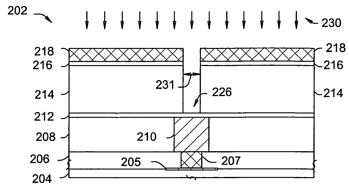
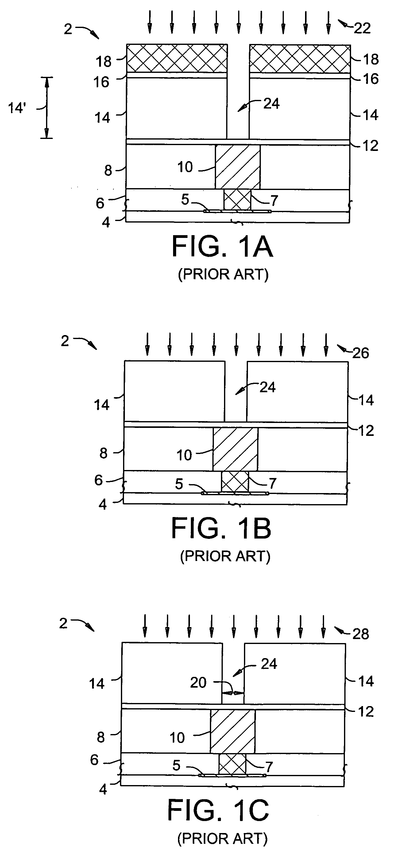
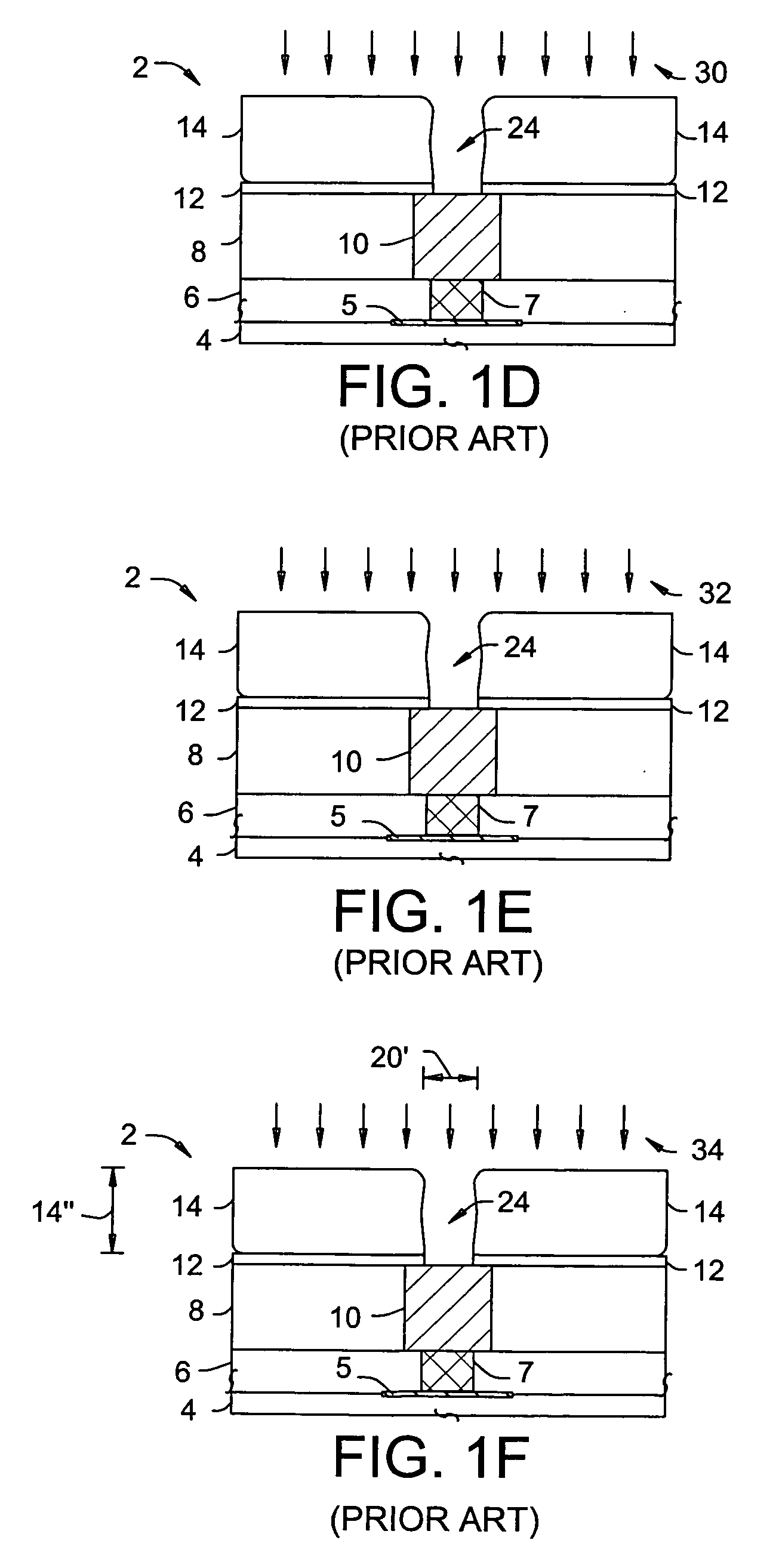
[0026] The present invention will now be described with reference to the attached drawings, wherein like reference numerals are used to refer to like elements throughout, and wherein the various structures are not necessarily drawn to scale. In the following description, for purposes of explanation, numerous specific details are set forth in order to provide a thorough understanding of one or more aspects of the present invention. It may be evident, however, that one or more aspects of the present invention may be practiced with a lesser degree of these specific details. In other instances, well-known structures and devices are shown in block diagram form in order to facilitate describing one or more aspects of the present invention.

[0027] One or more aspects of the present invention relate to forming single and / or dual damascene interconnect structures, including via and / or trench cavities or openings during interconnect processing of integrated circuits and other semiconductor de...


PUM


Abstract

One or more aspects of the subject disclosure pertain to forming single or dual damascene interconnect structures in the fabrication of semiconductor devices. The interconnect structures are formed in manners that mitigate one or more adverse effects associated with conventional techniques. One or more aspects of the invention may be employed, for example, to facilitate better via critical dimension (CD) control, improve selectivity of etch-stop layer to inter layer dielectric (ILD) and / or intra-metal dielectric (IMD) material, and / or to simplify and make the fabrication process more efficient and / or cost effective.

Description

RELATED APPLICATIONS [0001] This application is related to U.S. patent application Ser. No. 10 / 313,491, (Attorney Docket No. TI-34486), filed on Dec. 5, 2002, entitled “METHODS FOR FORMING SINGLE DAMASCENE VIA OR TRENCH CAVITIES AND FOR FORMING DUAL DAMASCENE VIA CAVITIES”, the entirety of which is hereby fully incorporated by reference.FIELD OF INVENTION [0002] The present invention relates generally to semiconductor processing and more particularly to implementing in-situ ashing in association with damascene processing in forming interconnect structures in the fabrication of semiconductor devices. BACKGROUND OF THE INVENTION [0003] In the manufacture of semiconductor products such as integrated circuits, individual electrical devices are formed on or in a semiconductor substrate, and are thereafter interconnected to form electrical circuits. Interconnection of these devices is typically accomplished by forming a multi-level interconnect network structure in layers formed over the ...

Claims


Application Information

Patent Timeline
IPC IPC(8): H01L21/4763H01L21/768
CPCH01L21/76808H01L21/76807
Inventor JIANG, PINGKRAFT, ROBERT
Owner TEXAS INSTR INC
Why Eureka
Try Eureka