

Method for thinning substrate of EL device
a technology of el and substrate, which is applied in the manufacture of electrode systems, cold cathode manufacturing, electric discharge tube/lamp manufacture, etc., can solve the problems of film-sealed el element portion being exposed to etching liquid and thereby damaged, and achieves the effect of reducing the operability of manufacture and thinning the substra
- Summary
- Abstract
- Description
- Claims
- Application Information
AI Technical Summary
Benefits of technology
Problems solved by technology
Method used
Image

Examples
Embodiment Construction
[0016] An embodiment of the present invention will be hereinafter described with reference to the accompanying drawings.
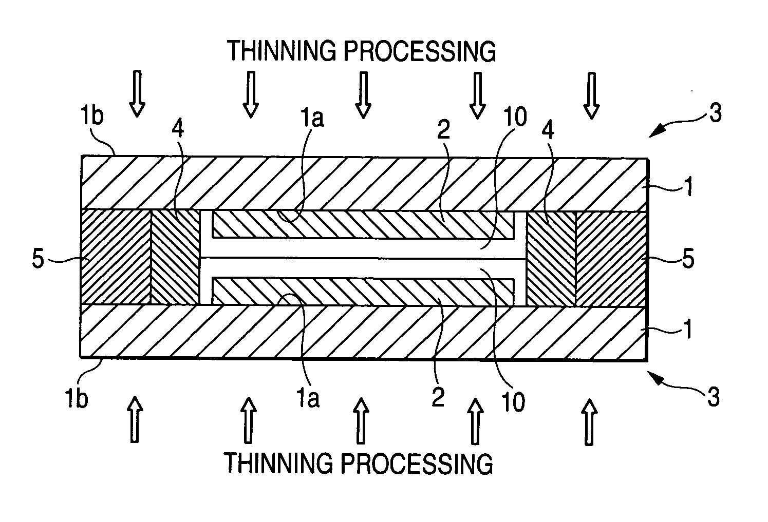
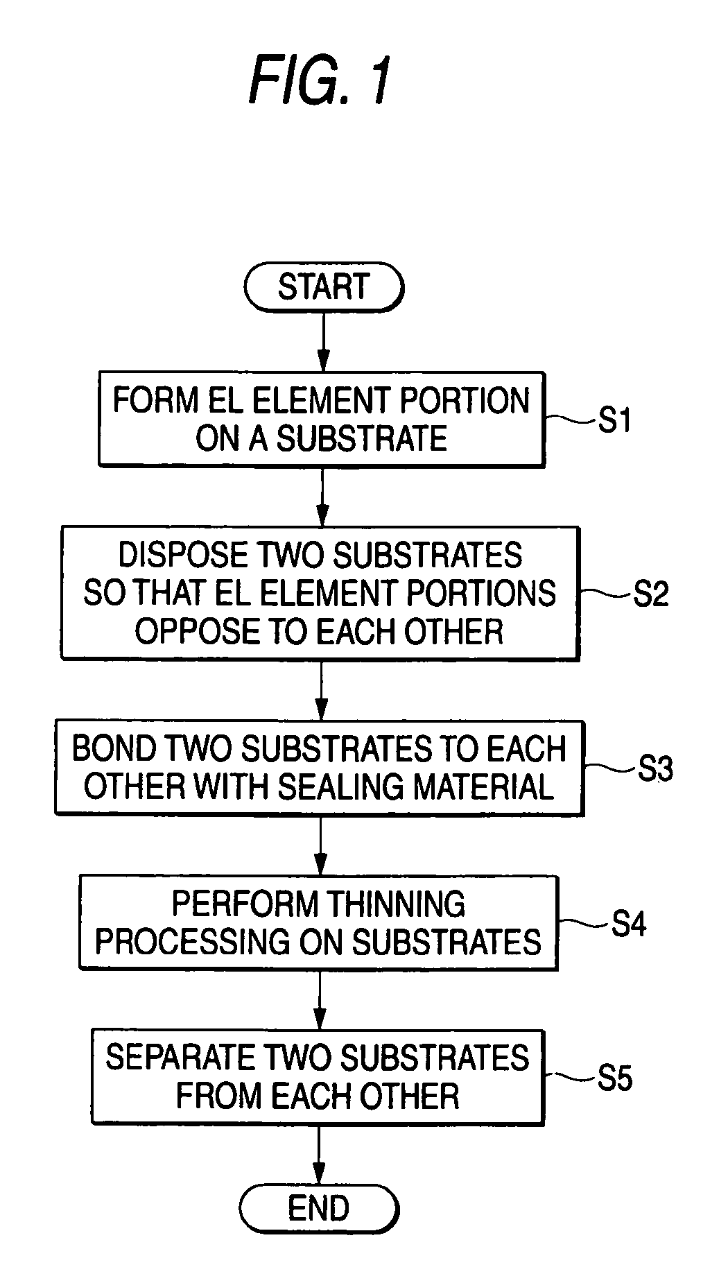
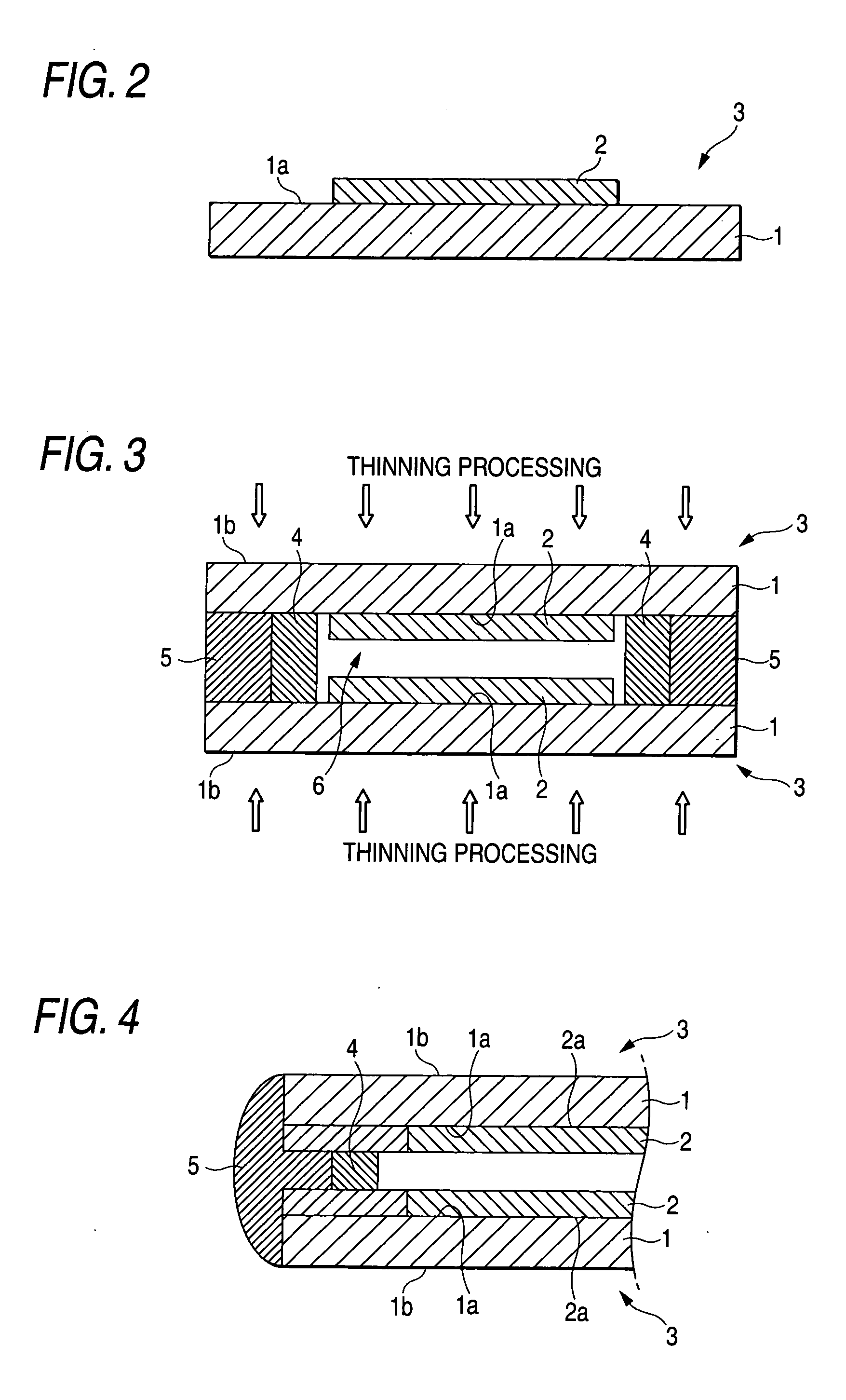
[0017] A method for thinning the substrate of an EL device according to the embodiment of the invention will be described with reference to a flowchart of FIG. 1. First, at step S1, an EL device 3 is formed by forming a film of an EL (electroluminescence) element portion 2 on a front surface 1a of a glass substrate 1 by a known method as shown in FIG. 2. The EL element portion 2 has a pair of electrode layers and a light-emitting layer that is interposed between the two electrode layers. To prevent entrance of external water, gas, etc., the two electrode layers and the light-emitting layer are sealed with a film. The EL element portion 2 is smaller in size than the glass substrate 1, and the front surface 1a of the glass substrate 1 has an exposed portion around the EL element portion 2. Terminals etc. (not shown) for external connections are formed in a periphera...
PUM
 Abstract
Description
Claims
Application Information