Mechanical oscillator for wafer scan with spot beam

a mechanical oscillator and spot beam technology, applied in the field of semiconductor processing systems, can solve the problems of difficult to achieve uniform translation and/or rotation, large size of ion implanters, complex and/or long beam lines

Inactive Publication Date: 2005-11-10
AXCELIS TECHNOLOGIES
View PDF15 Cites 5 Cited by
  • Summary
  • Abstract
  • Description
  • Claims
  • Application Information

AI Technical Summary

Benefits of technology

[0005] The present invention overcomes the limitations of the prior art. Consequently, the following presents a simplified summary of the invention in order to provide a basic understanding of some aspects of the invention. This summary is not an extensive overview of the...

Problems solved by technology

Processing batches of substrates in such a manner, however, generally makes the ion implanter substantially large in size.
The process of scanning or shaping a uniform ion beam, however, generally requires a complex and/or long beam line, which is gene...

Method used


Image

  • Mechanical oscillator for wafer scan with spot beam
  • Mechanical oscillator for wafer scan with spot beam
  • Mechanical oscillator for wafer scan with spot beam

Examples


Embodiment Construction

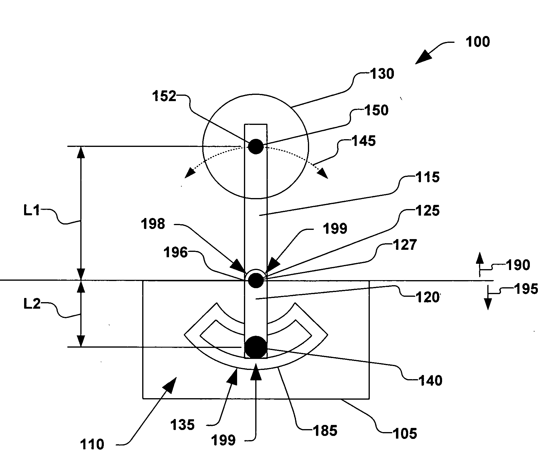
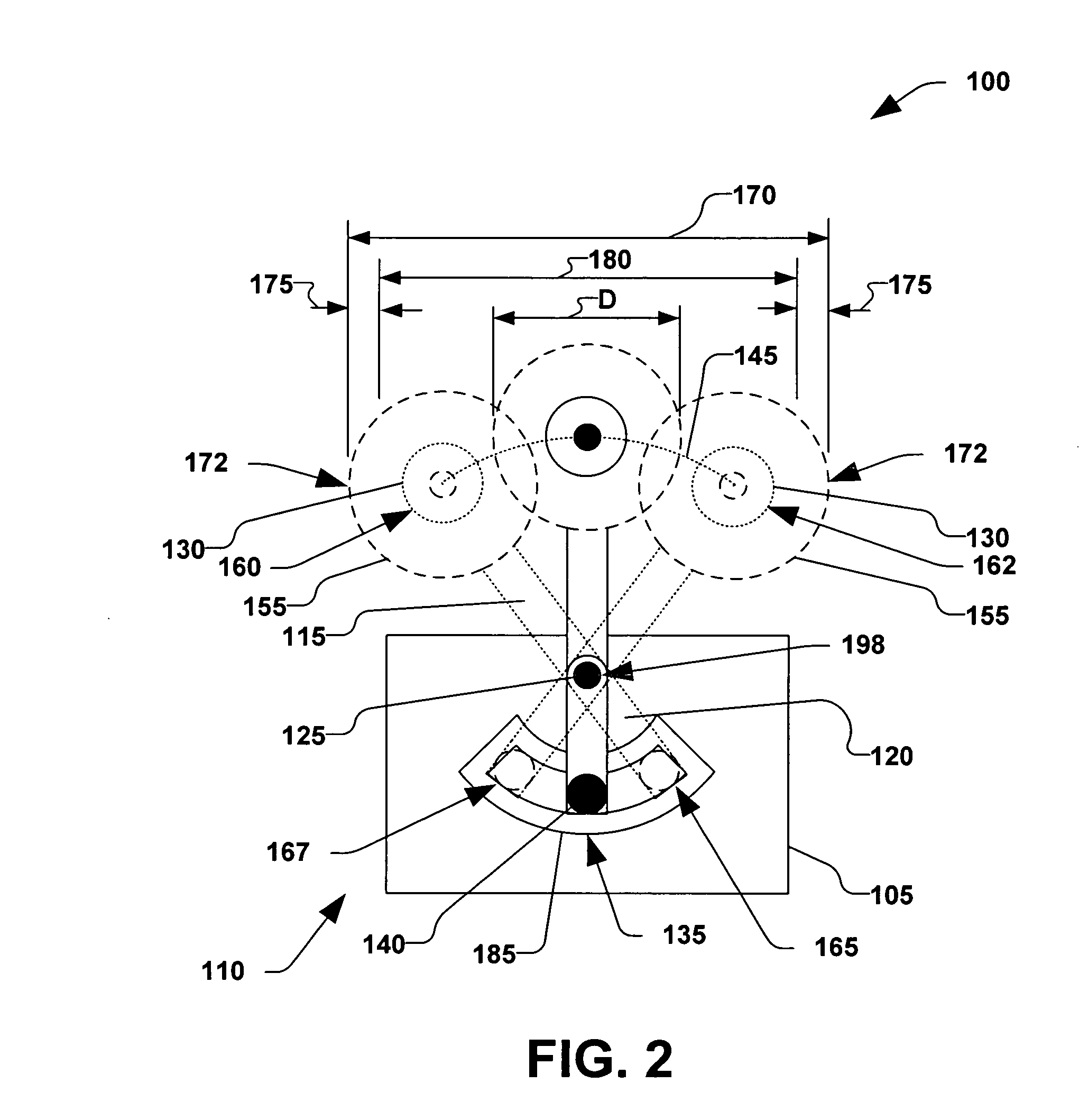
[0025] The present invention is directed generally towards a scanning apparatus for moving a substrate relative to a beam. More particularly, the scanning apparatus is operable to translate the substrate at a generally constant velocity with respect to a spot beam within a predetermined scan range, wherein a motion of the scanning apparatus oscillates via a cantilevered arm coupled to a translational actuator. Accordingly, the present invention will now be described with reference to the drawings, wherein like reference numerals are used to refer to like elements throughout. It should be understood that the description of these aspects are merely illustrative and that they should not be taken in a limiting sense. In the following description, for purposes of explanation, numerous specific details are set forth in order to provide a thorough understanding of the present invention. It will be evident to one skilled in the art, however, that the present invention may be practiced witho...


PUM


Abstract

The present invention is directed to a scanning apparatus and method for processing a substrate, wherein the scanning apparatus comprises a first link and a second link rigidly coupled to one another at a first joint, wherein the first link and second link are rotatably coupled to a base portion by the first joint, therein defining a first axis. An end effector, whereon the substrate resides, is coupled to the first link. The second link is coupled to a first actuator via at least second joint. The first actuator is operable to translate the second joint with respect to the base portion, therein rotating the first and second links about the first axis and translating the substrate along a first scan path in an oscillatory manner. A controller is further operable to maintain a generally constant translational velocity of the end effector within a predetermined scanning range.

Description

FIELD OF THE INVENTION [0001] The present invention relates generally to semiconductor processing systems, and more specifically to an apparatus and method for controlling a quality and precision of motion of a substrate during ion implantation. BACKGROUND OF THE INVENTION [0002] In the semiconductor industry, various manufacturing processes are typically carried out on a substrate (e.g., a semiconductor wafer) in order to achieve various results thereon. Processes such as ion implantation, for example, can be performed in order to obtain a particular characteristic on or within the substrate, such as limiting a diffusivity of a dielectric layer on the substrate by implanting a specific type of ion. Conventionally, ion implantation processes are performed in either a batch process, wherein multiple substrates are processed concurrently, or a serial process, wherein a single substrate is individually processed. Traditional high-energy or high-current batch ion implanters, for example...

Claims


Application Information

Patent Timeline
IPC IPC(8): H01L21/00H01L21/687
CPCH01J37/3171H01L21/68764H01L21/67069H01J2237/20228
Inventor ASDIGHA, MEHRANCLEVELAND, KURT D.KRISHNASAMY, JAYOTA, KAN
Owner AXCELIS TECHNOLOGIES
Why Eureka
Try Eureka