Thin film piezoelectric resonator and manufacturing process thereof

a piezoelectric resonator and film technology, applied in the direction of piezoelectric/electrostrictive device details, device material selection, device details, etc., can solve the problems of easy current leakage and wire breakage, ruined flatness and cleanliness, and difficult to accurately process the transducer

Active Publication Date: 2005-11-10
KK TOSHIBA
View PDF14 Cites 91 Cited by
  • Summary
  • Abstract
  • Description
  • Claims
  • Application Information

AI Technical Summary

Problems solved by technology

However, such narrow pitch makes it difficult to accurately process the transducers, and causes current leakage and breaking of wire easily when high-power signals enter the transducers.
This exposure causes the adsorption of impurities such as oxygen to the surface of the lower electrode layer 804, so that the flatness and cleanliness are ruined.
Such low film quality causes low quality of a single thin film piezoelectric resonator and uneven quality between thin film piezoelectric resonators.

Method used


Image

  • Thin film piezoelectric resonator and manufacturing process thereof
  • Thin film piezoelectric resonator and manufacturing process thereof
  • Thin film piezoelectric resonator and manufacturing process thereof

Examples


first embodiment

[0031] A thin film piezoelectric resonator characteristically, includes a lower electrode layer and a piezoelectric thin film that are both deposited continuously and patterned with a common mask to form the same shape. Besides, the thin film piezoelectric resonator, characteristically, includes an insulating film that is located on a part of the top face of the piezoelectric thin film, one of the sides of the lower electrode layer, and one of the sides of the piezoelectric thin film in the plane where the one of the sides of the lower electrode layer is located, and includes an upper electrode layer that is located on the surface of the insulating film and a part of the top face of the piezoelectric thin film.

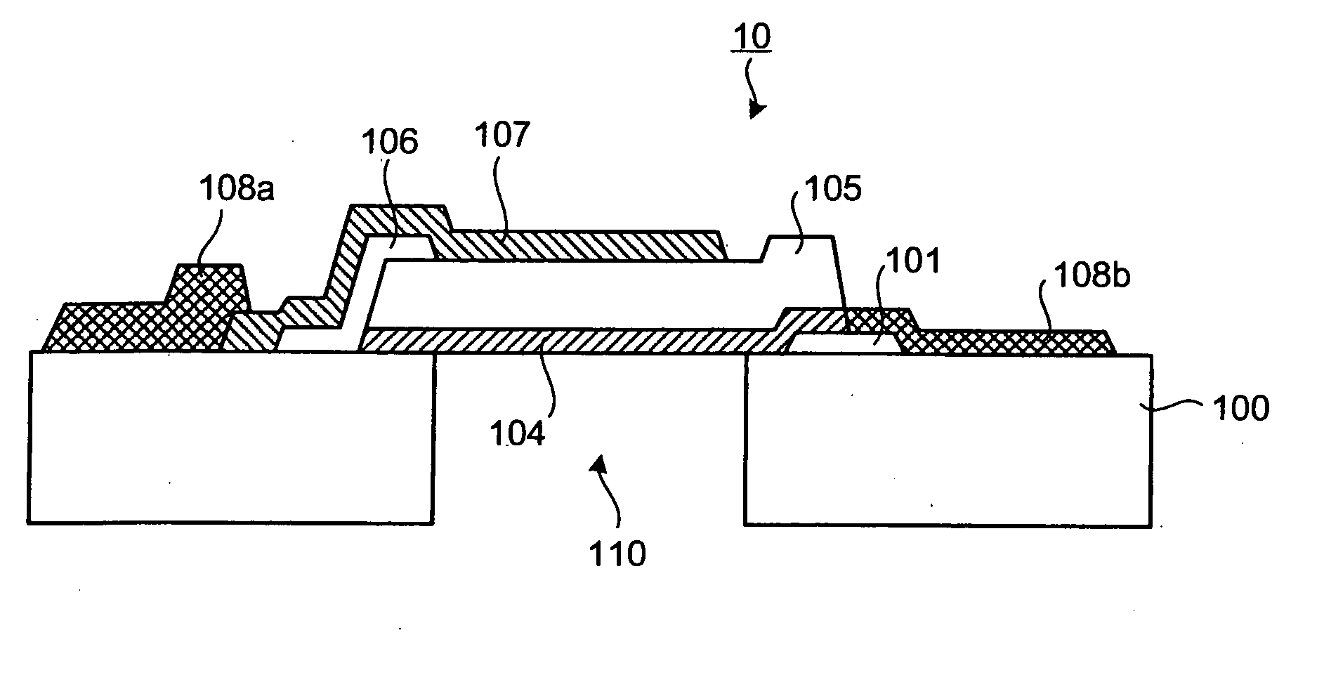
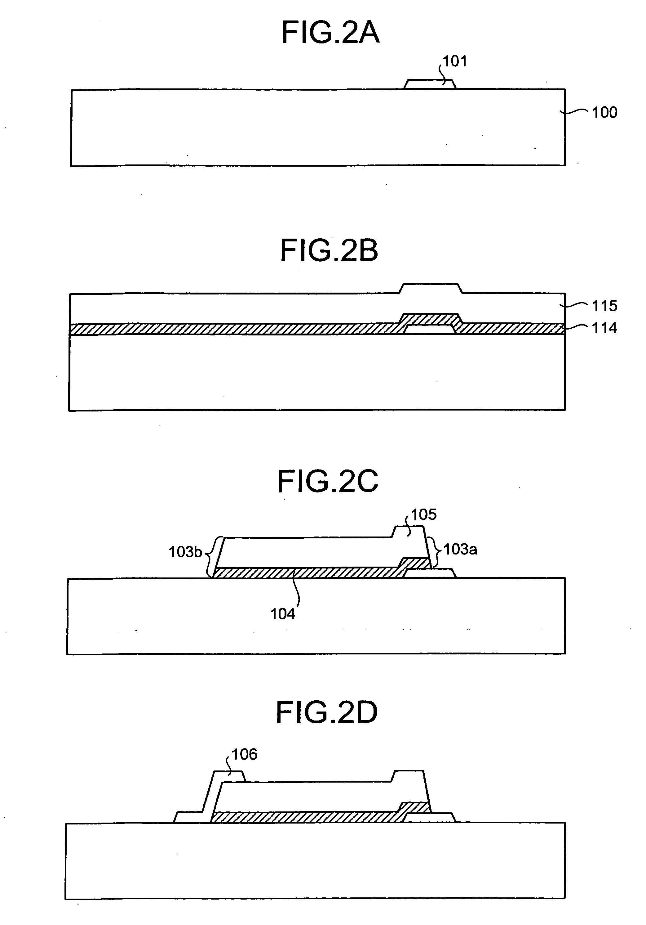
[0032]FIG. 1 is a cross section of a thin film piezoelectric resonator according to a first embodiment. A thin film piezoelectric resonator 10 in FIG. 1 has a structure in which a lower electrode layer 104, a piezoelectric thin film 105, and an upper electrode layer 107 are s...

second embodiment

[0042] A thin film piezoelectric resonator is characterized in that the insulating film that insulates between the upper electrode layer and the lower electrode layer are formed only on one of the sides of the piezoelectric thin film, one of the sides of the lower electrode layer in the same plane where the one of the sides of the piezoelectric thin film is located, and a part of the silicon substrate. In other words, a part of the insulating film 106 shown in FIG. 1, formed on the piezoelectric thin film 105 is removed.

[0043]FIG. 5 is a cross section of a thin film piezoelectric resonator according to a second embodiment. As for a silicon substrate 200 in FIG. 5, a dummy pad 201, a lower electrode layer 204, a piezoelectric thin film 205, electrode pads 208a and 208b, and a cavity 210 correspond to the silicon substrate 100, the dummy pad 101, the lower electrode layer 104, the piezoelectric thin film 105, the electrode pads 108a and 108b, and the cavity 110 shown in FIG. 1, respe...

third embodiment

[0047] A thin film piezoelectric resonator characteristically, includes a lower electrode layer and a first piezoelectric thin film that are both deposited continuously and patterned with a common mask to form the same shape, and also includes a second piezoelectric thin film that covers the first piezoelectric thin film.

[0048]FIG. 6 is a cross section of a thin film piezoelectric resonator according to a third embodiment. A thin film piezoelectric resonator 30 in FIG. 6 has a structure in which a lower electrode layer 304, a first piezoelectric thin film 305a, a second piezoelectric thin film 305b, and an upper electrode layer 307 are sequentially formed on a silicon substrate 300. On the silicon substrate 300, an electroconductive dummy pad 301 for electrically connecting between the lower electrode layer 304 and an electrode pad 308b is formed. The sides of the lower electrode layer 304 and the sides of the first piezoelectric thin film 305a are located in the same plane. The se...


PUM


Abstract

a thin film piezoelectric resonator includes a substrate having a cavity, and a resonance portion located on the substrate and right above the cavity. The resonance portion includes a lower electrode layer located at a side of the cavity, an upper electrode layer opposite to the lower electrode layer, and a piezoelectric thin film located between the upper electrode layer and the lower electrode layer. A side of the piezoelectric thin film and a side of the lower electrode layer are located in a common plane.

Description

CROSS-REFERENCE TO RELATED APPLICATIONS [0001] This application is based upon and claims the benefit of priority from Japanese Patent Application No. 2004-136135, filed on Apr. 30, 2004; the entire contents of which are incorporated herein by reference. BACKGROUND OF THE INVENTION [0002] 1. Field of the Invention [0003] The present invention relates to a thin film piezoelectric resonator, which can be used as a high frequency filter or an RF oscillator, and a method of manufacturing the resonator. [0004] 2. Description of the Related Art [0005] Surface acoustic wave (SAW) devices, which have advantages in their high resonance quality factors and their miniaturization, are rapidly developed to be used in filter applications such as LC or dielectric bandpass filters. The SAW device basically has a piezoelectric substrate of single crystal material, and two interdigital transducers located thereon. The resonance frequency of such a SAW device is in inverse proportion to the pitch of an...

Claims


Application Information

Patent Timeline
Patent Type & Authority Applications(United States)
IPC IPC(8): H01L41/09H01L41/04H01L41/08H01L41/18H01L41/22H01L41/23H01L41/29H01L41/332H03H3/02H03H9/17
CPCH03H3/02H03H2003/023H03H9/174
Inventor ITAYA, KAZUHIKOKAWAKUBO, TAKASHISANO, KENYAOHARA, RYOICHI
Owner KK TOSHIBA
Why Eureka
Try Eureka