Substrate for liquid crystal display and liquid crystal display having the same

Inactive Publication Date: 2005-11-10
SHARP KK
View PDF7 Cites 13 Cited by
  • Summary
  • Abstract
  • Description
  • Claims
  • Application Information

AI Technical Summary

Benefits of technology

[0022] It is an object of the invention to provide a liquid crystal display which can be manufactured through simpl

Problems solved by technology

This results in a problem in that processes for manufacturing the TFT substrate 102 become complicated to reduce productivity.
Problems also arise in that the resolution of patterning is reduced and in that undeveloped regions can remain.
In the case of the liquid crystal display having alignment regulating structures, since the aperture rati

Method used


Image

  • Substrate for liquid crystal display and liquid crystal display having the same
  • Substrate for liquid crystal display and liquid crystal display having the same
  • Substrate for liquid crystal display and liquid crystal display having the same

Examples


Example

[First Embodiment]

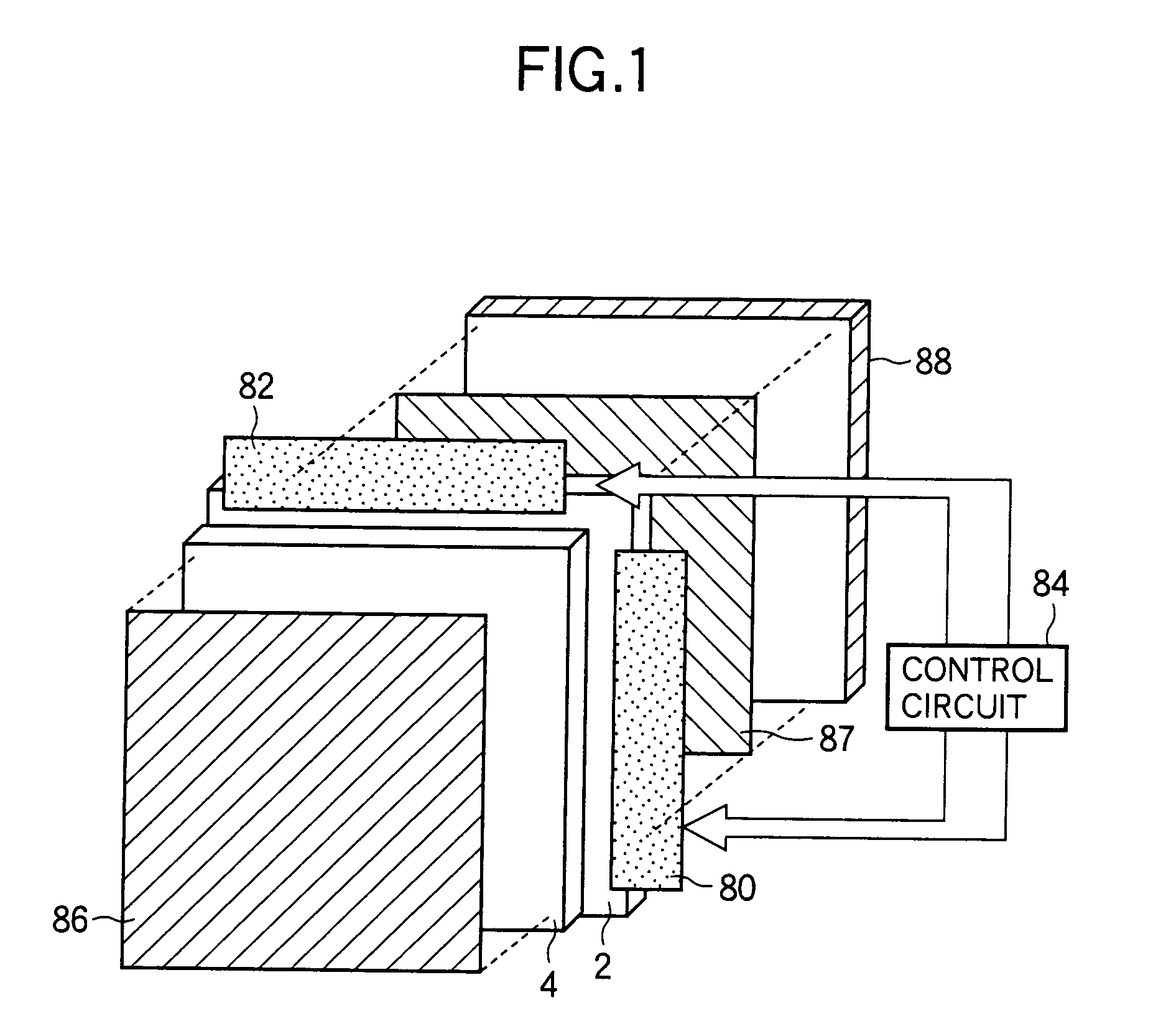
[0050] A description will now be made with reference to FIGS. 1 to 7 on a substrate for a liquid crystal display and a liquid crystal display having the same according to an embodiment of the invention. FIG. 1 shows a schematic configuration of a liquid crystal display according to the present embodiment. As shown in FIG. 1, the liquid crystal display has structure in which a TFT substrate (base substrate) 2 having a pixel electrode and a TFT formed in each of pixel regions and an opposite substrate 4 having a common electrode formed thereon are combined in a face-to-face relationship to seal a liquid crystal between them. Alignment films for aligning liquid crystal molecules in a predetermined direction are formed on surfaces of the substrates 2 and 4 opposite to each other.

[0051] The TFT substrate 2 is provided with a gate bus line driving circuit 80 having driver ICs for driving the plurality of gate bus lines mounted thereon and a drain bus line driving circu...

Example

[Second Embodiment]

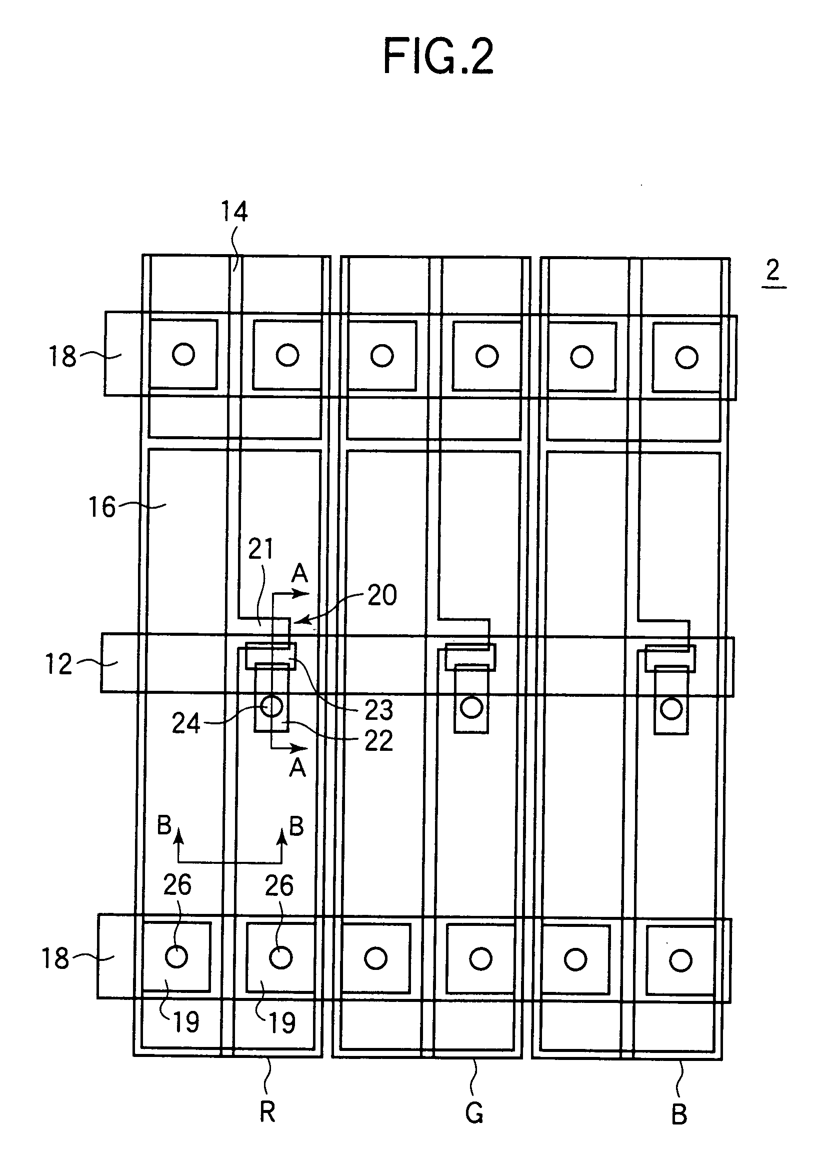
[0061] A description will now be made with reference to FIGS. 8 to 10 on a substrate for a liquid crystal display according to a second embodiment of the invention. FIG. 8 shows a configuration of a TFT substrate (base substrate) according to the present embodiment. As shown in FIG. 8, a TFT substrate 2 has a plurality of protrusions 40 to serve as alignment regulating structures and constitutes one of substrates of an MVA normally black mode liquid crystal display, for example. For example, the protrusions 40 are formed of a resist and are in a substantially circular configuration when viewed in a direction perpendicular to a surface of the substrate. The protrusions 40 are provided above positions where gate bus lines 12 and drain bus lines 14 intersect each other and above positions where storage capacitor bus lines 18 and the drain bus lines 14 intersect each other.

[0062] In the present embodiment, the protrusions 40 are formed in regions that do not contrib...

Example

[Third Embodiment]

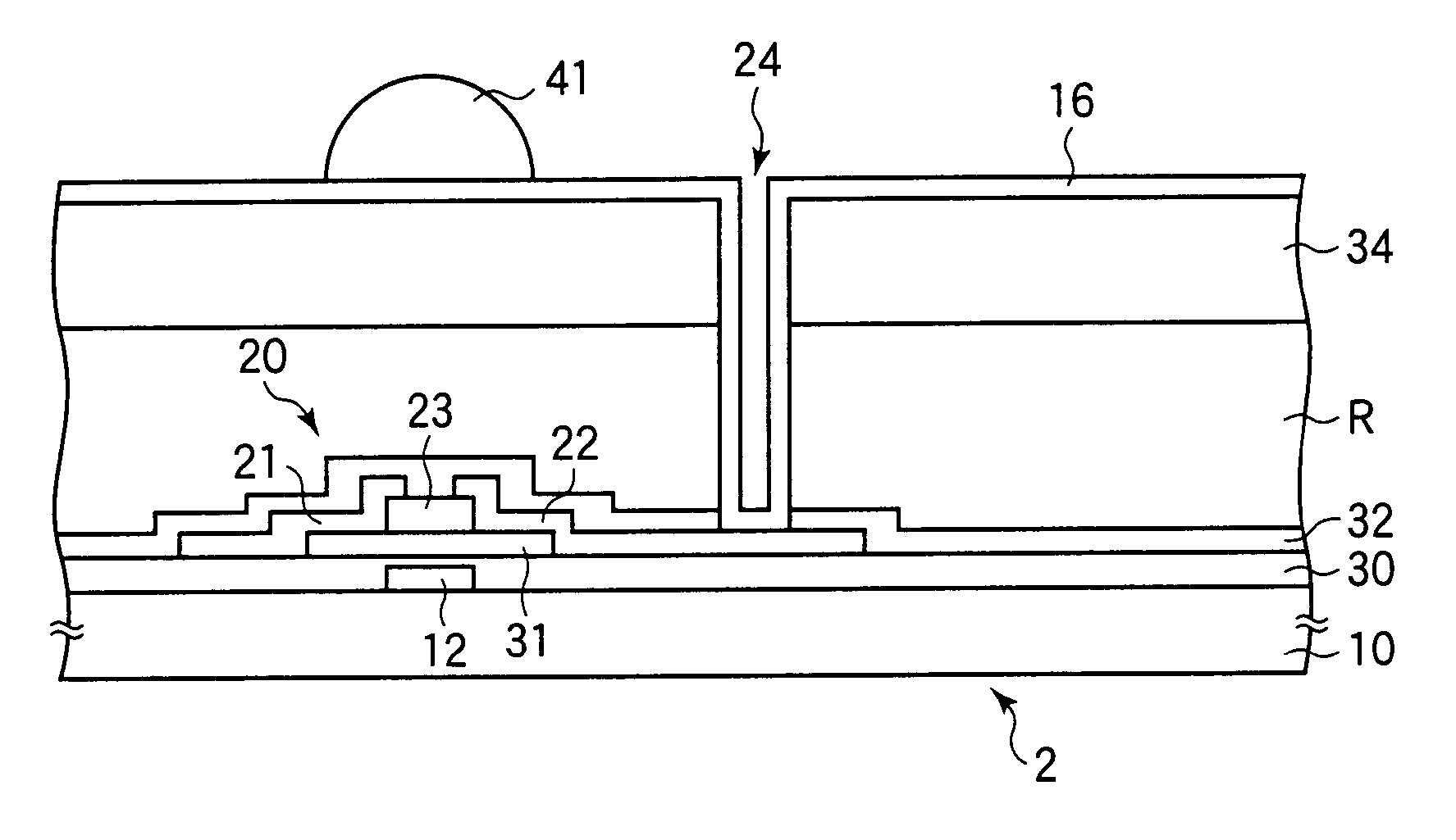
[0065] A description will now be made with reference to FIGS. 11 to 18B on a substrate for a liquid crystal display according to a third embodiment of the invention. FIG. 11 shows a configuration of a TFT substrate (base substrate) according to the present embodiment, and FIG. 12 shows a configuration of a section of the TFT substrate along the line D-D in FIG. 11. As shown in FIGS. 11 and 12, the TFT substrate 2 has a transparent electrode 15 made of a light-transmitting electrode material and a reflective electrode 17 made of a light-reflecting electrode material in each pixel and constitutes one of substrates of a transflective liquid crystal display. The transparent electrodes 15 and the reflective electrodes 17 in one pixel are electrically connected to each other. The transparent electrodes 15 transmit light impinging thereupon from a backlight unit 88 provided on a backside of the TFT substrate 2 toward a top side of the same, and the reflective electrode 1...


PUM


Abstract

The invention relates to a liquid crystal display used in a display section of an electronic apparatus and a liquid crystal display substrate used for the same and provides a liquid crystal display that can be manufactured through simplified manufacturing processes and that can provide high display quality and a liquid crystal display substrate used for the same. A configuration is employed which includes gate bus lines and drain bus lines formed on a substrate such that they intersect each other with an insulation film interposed therebetween and pixel electrodes provided so as to cover at least one of the gate bus lines and the drain bus lines with a dielectric layer interposed therebetween and forming parasitic capacities between the gate bus lines or drain bus lines and themselves.

Description

BACKGROUND OF THE INVENTION [0001] 1. Field of the Invention [0002] The present invention relates to a liquid crystal display used for a display section of an electronic apparatus and a substrate for a liquid crystal display used for such a display. [0003] 2. Description of the Related Art [0004] In general, an active matrix liquid crystal display has a TFT substrate on which a thin film transistor (TFT) is formed at each pixel as a switching element and an opposite substrate on which color filters (CF) are formed. [0005] The TFT substrate has gate bus lines and drain bus lines that intersect each other with an insulation film interposed therebetween. TFTs are formed in the vicinity of the positions where the bus lines intersect. A pixel electrode is formed at each of a plurality of pixel regions that are arranged in the form of a matrix. [0006] For example, the TFT substrate is patterned using the separate exposure method utilizing a stepper. According to the separate exposure meth...

Claims


Application Information

Patent Timeline
IPC IPC(8): G02F1/1368G02F1/1333G02F1/1335G02F1/1345G02F1/136G02F1/1362H01L29/786
CPCG02F1/133555G02F2001/13606G02F1/136227G02F1/13606G02F1/136
Inventor TAKAGI, TAKASHIHOSHINO, ATSUYUKISAWASAKI, MANABUSAGUCHI, TAKUYA
Owner SHARP KK
Why Eureka
Try Eureka